Image Attribution
Image attributions for images used on this website.
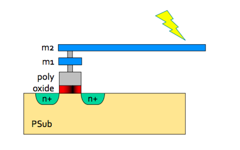 Image from Mohamed Shalan
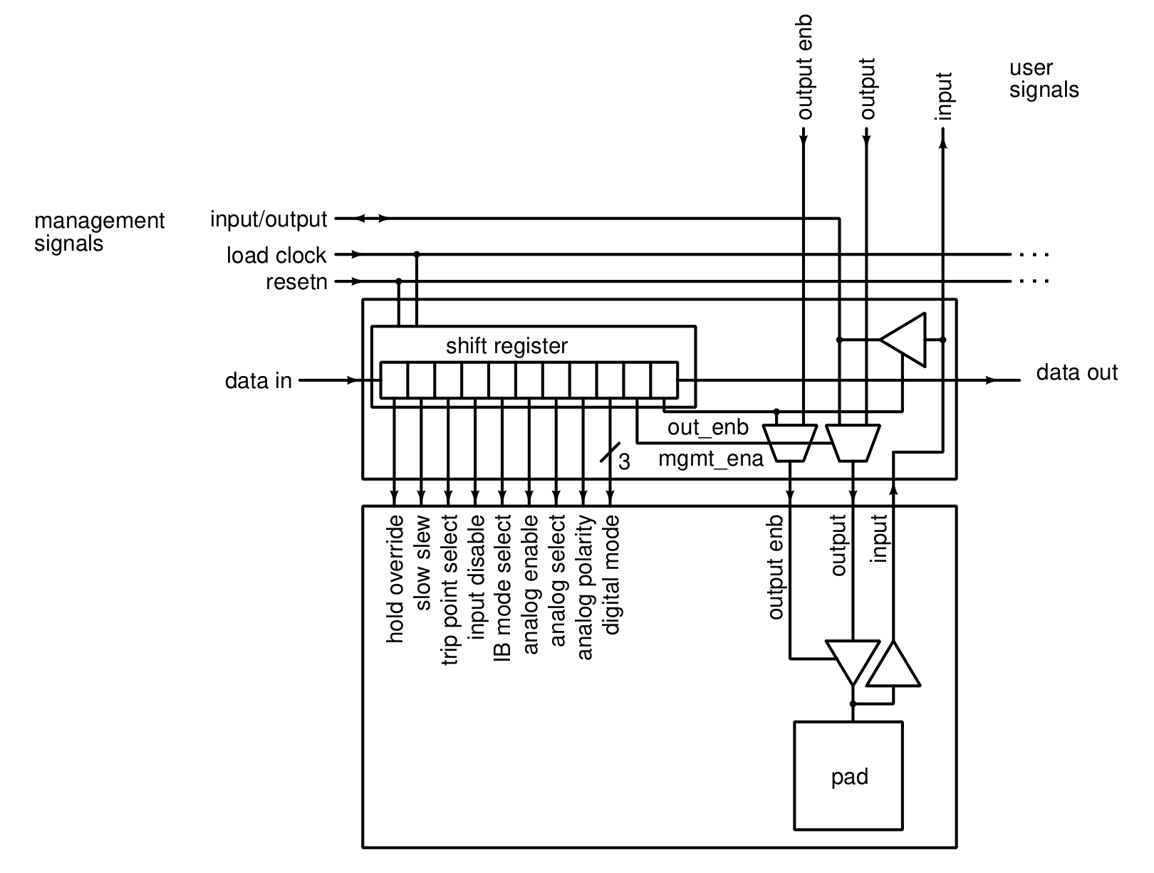 Image from Caravel Datasheet
 Image from RFCafe
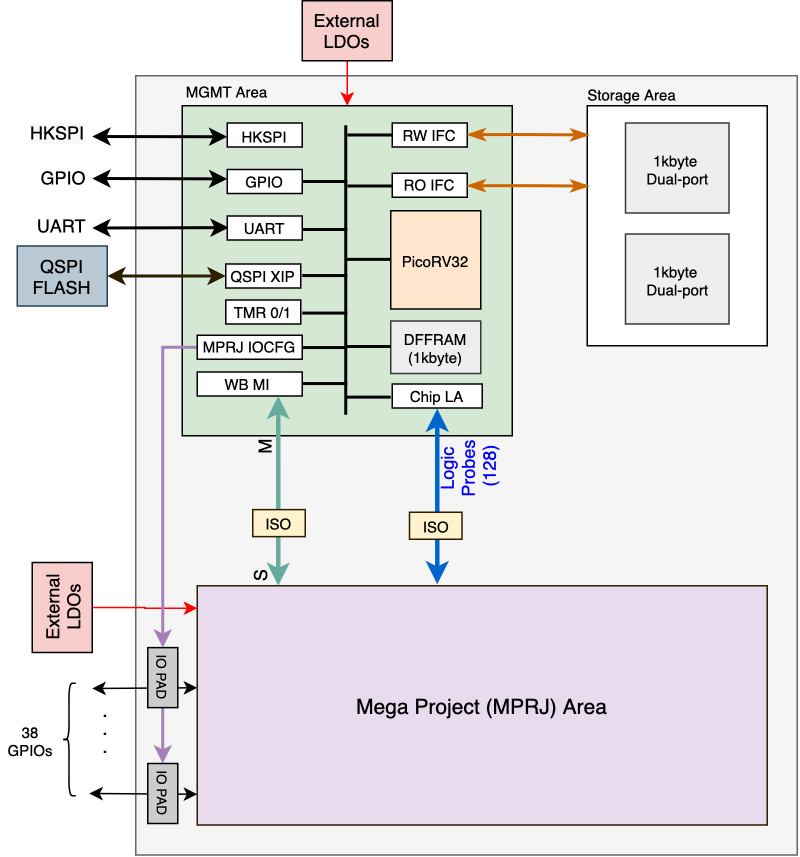 Image from Caravel Datasheet
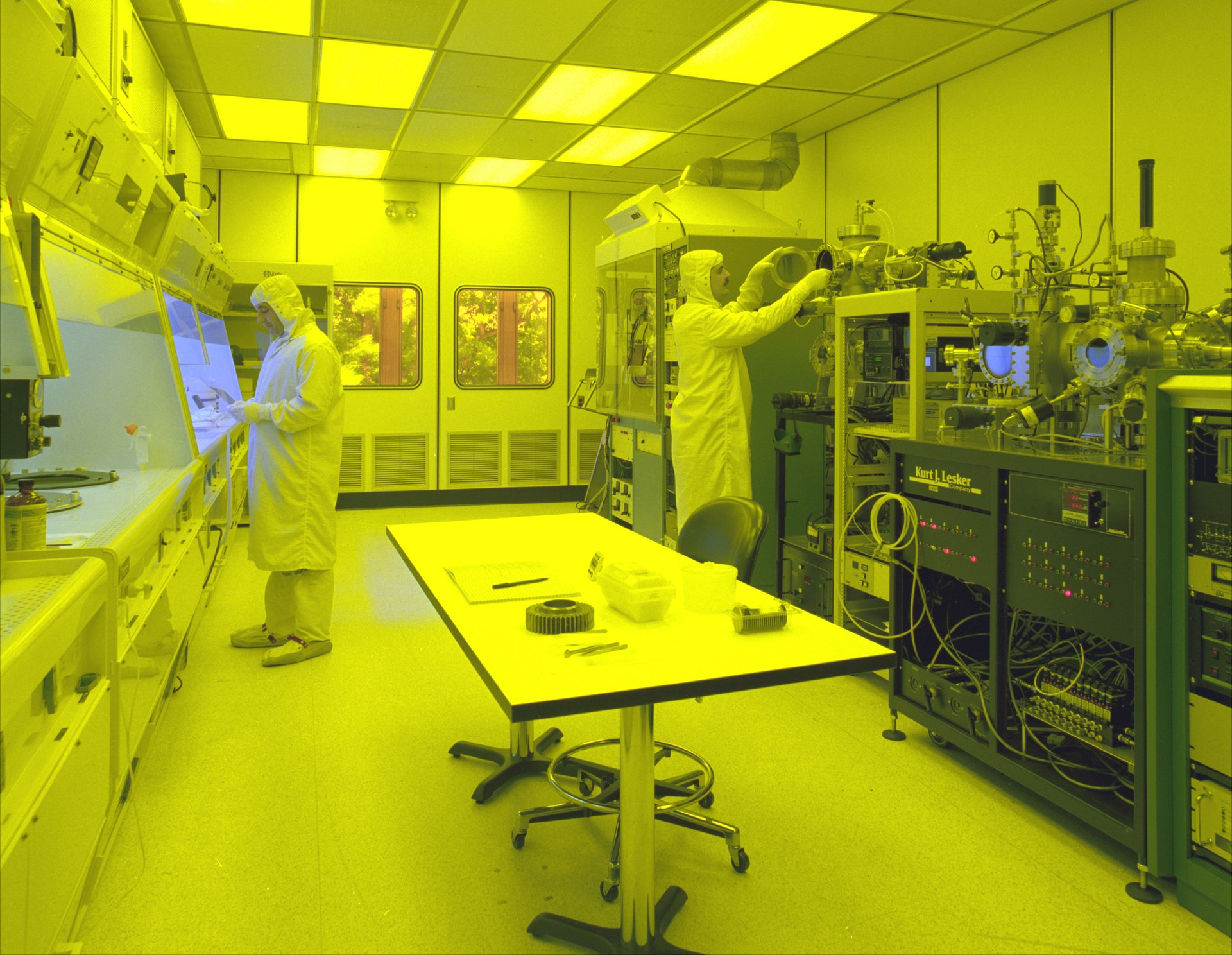 Image from Wikipedia
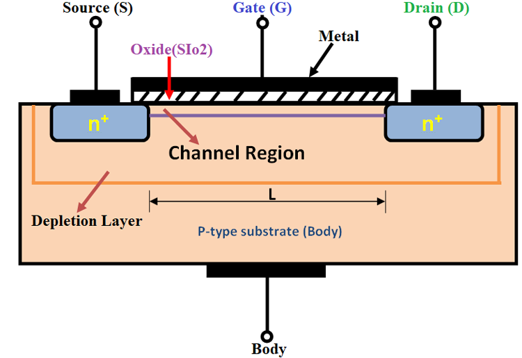 Image from Components 101
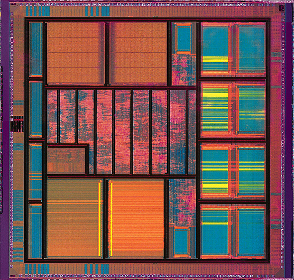 Image from Wikipedia
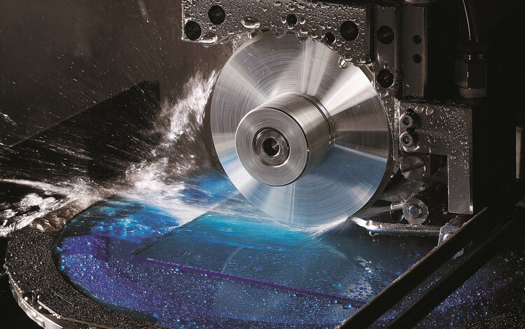 Image from WhaTech
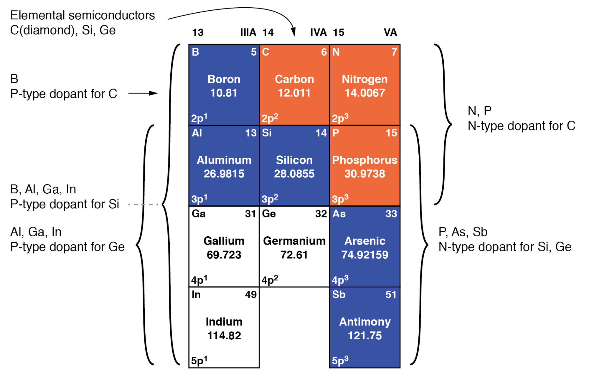 Image from Technocrazed
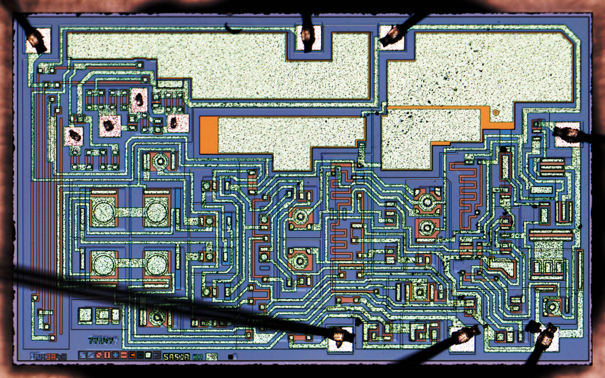 Image from Zeptobars
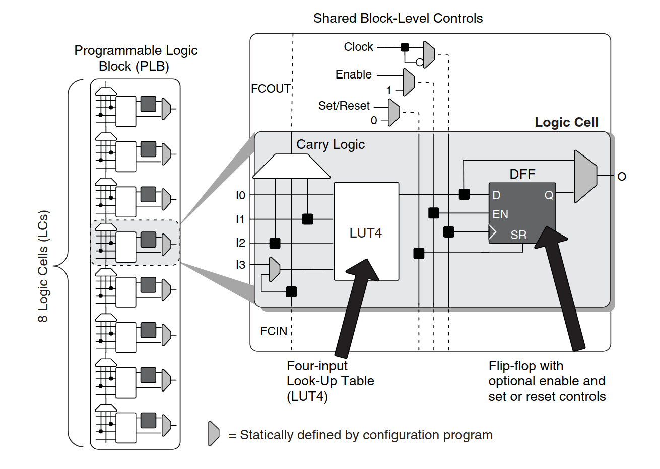 Image from Lattice Semiconductor
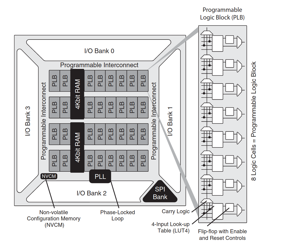 Image from Lattice Semiconductor
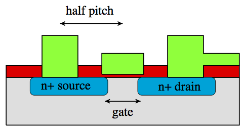 Image from M. Rovitto
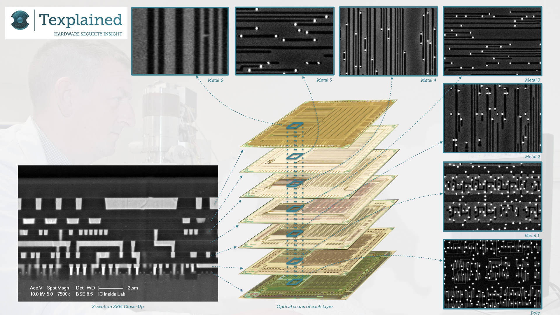 Image from Texplained
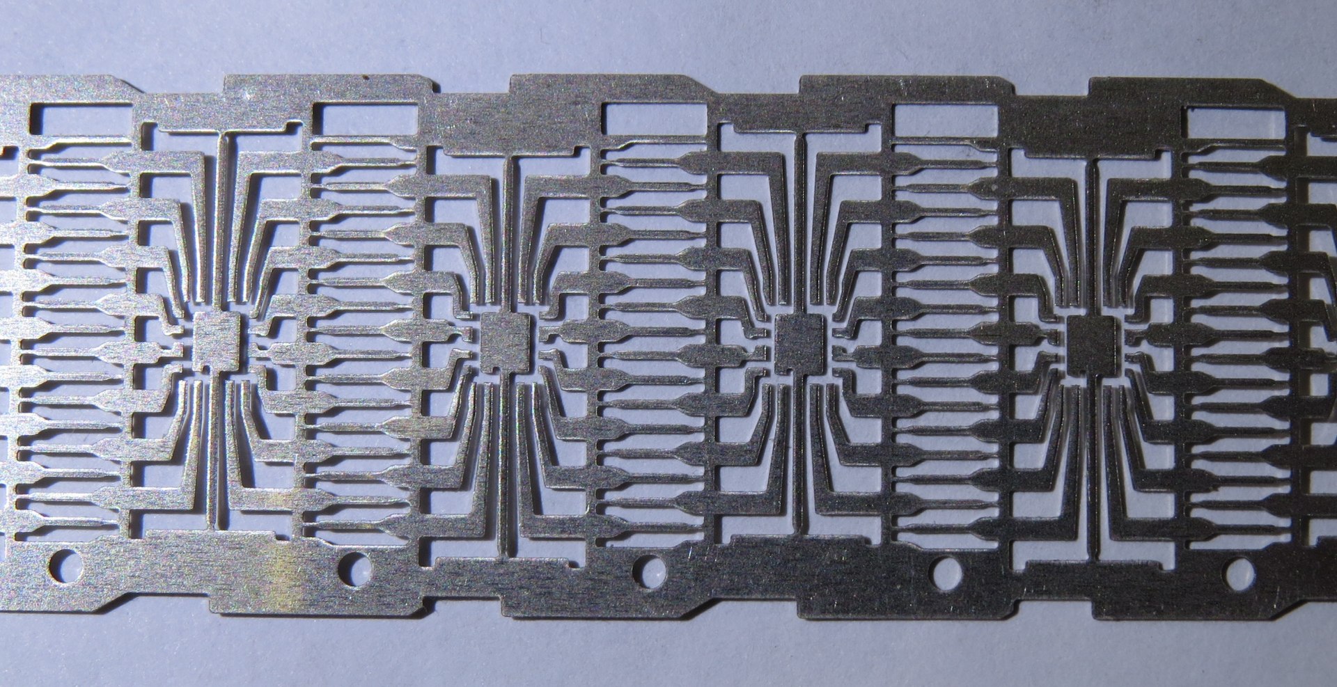 Image from Wikimedia
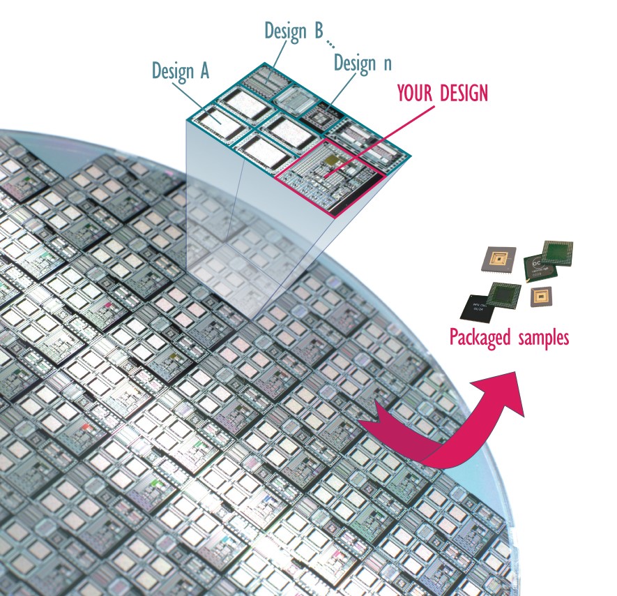 Image from Europractice
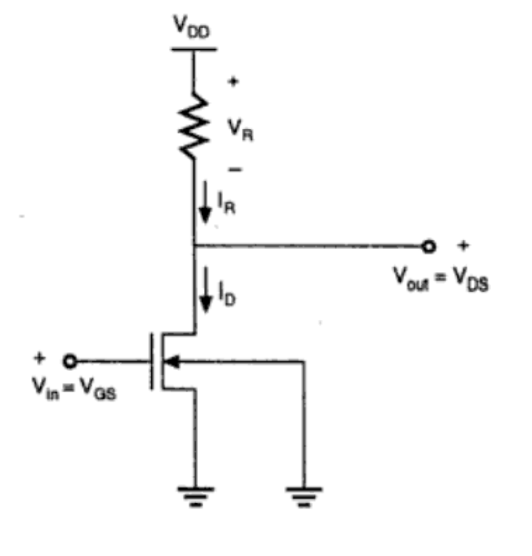 Image from VLSI Systems by Mead & Conway
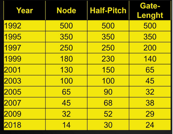 Image from der8auer youtube channel
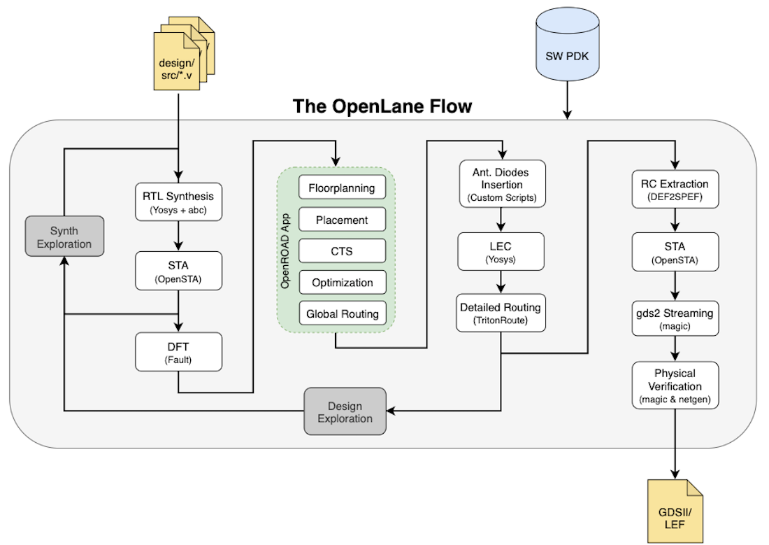 Image from LibreLane docs
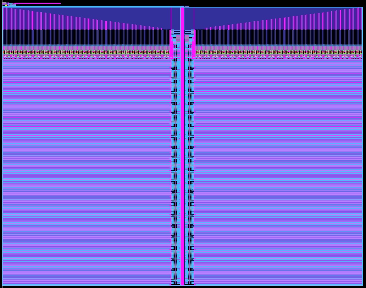 Image from OpenRAM
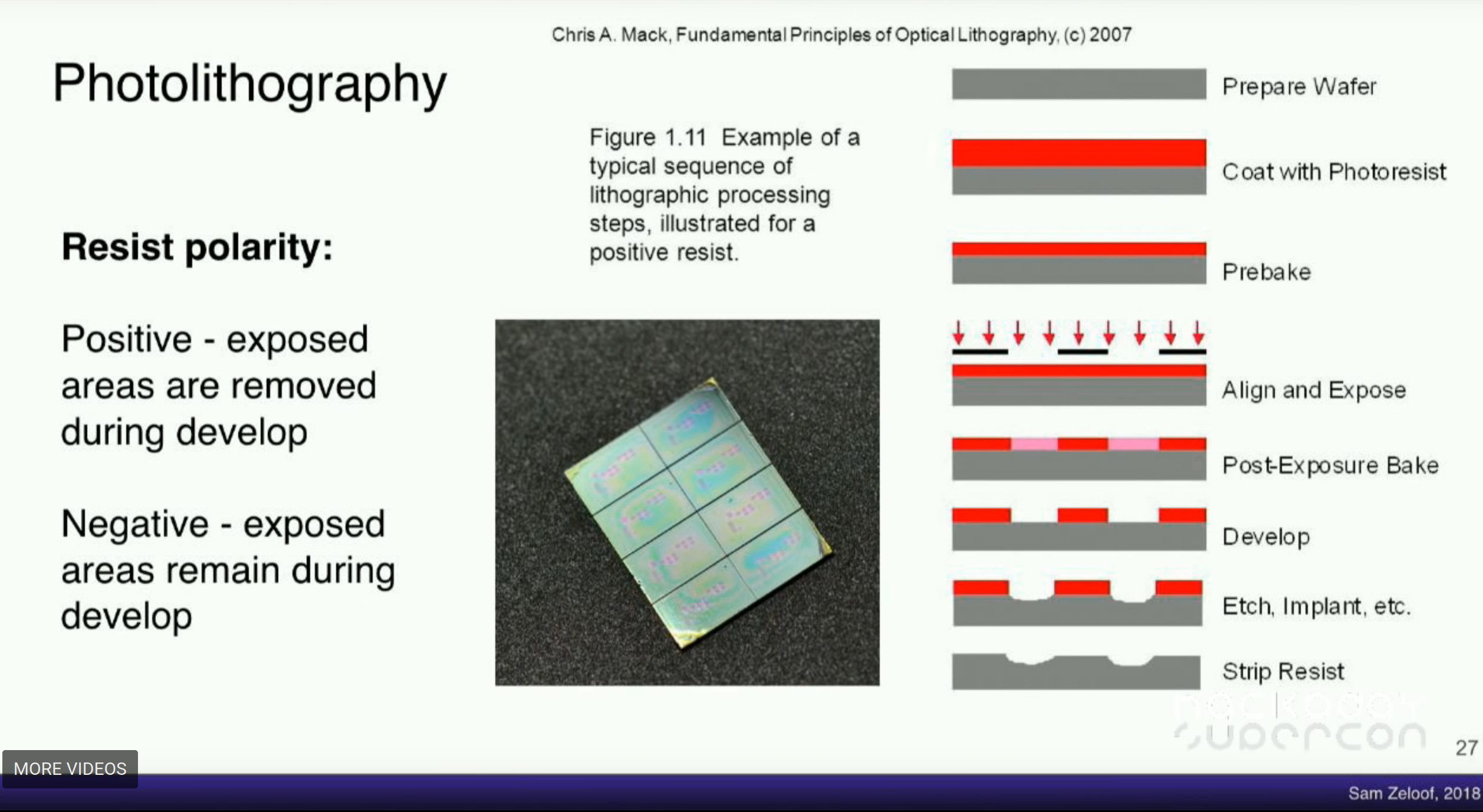 Image from Sam Zeloof’s supercon presentation
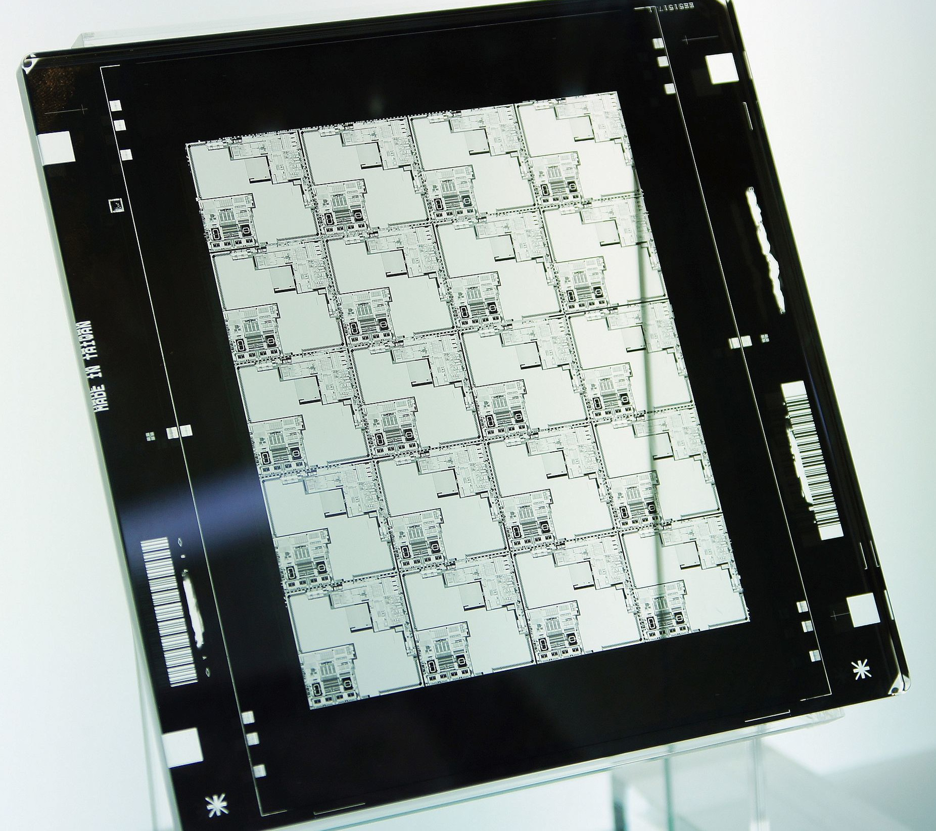 Image from Wikipedia
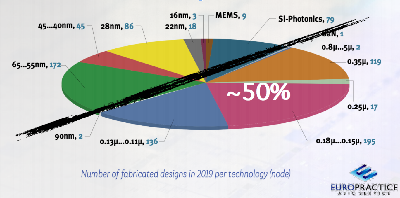 Image from Mohamed Kassem’s FOSSi presentation
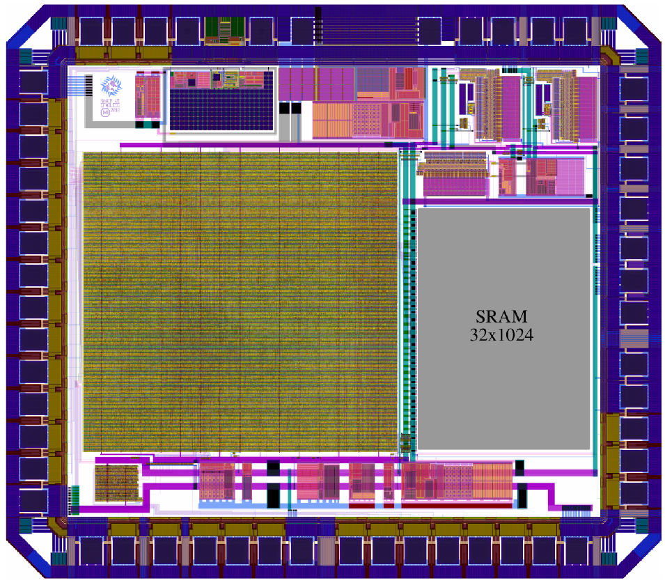 Image from Mohamed Kassem’s FOSSi presentation
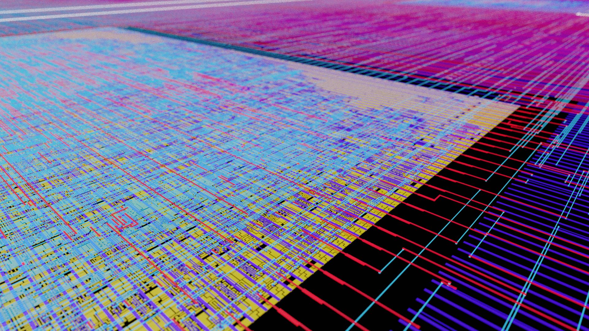 Images from course participant Maximo Balestrini.
some renders of the multi-project design presented by @matthewvenn for the @Google , @efabless & @SkyWaterFoundry MPW2 (last photo is my square) pic.twitter.com/g7RhRQGI6J
— Maximo (@maxiborga) June 24, 2021
more ASIC renders of the multi-project design from the zero to ASIC course
— Maximo (@maxiborga) July 7, 2021
visible layers: li, m1, m2, m3 (m4 just for the highlighted activation lines) pic.twitter.com/OAw3TGHCCY
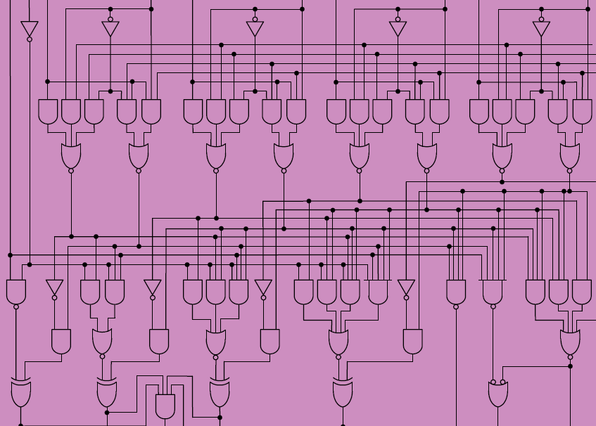 Image from VLSI Systems by Mead & Conway
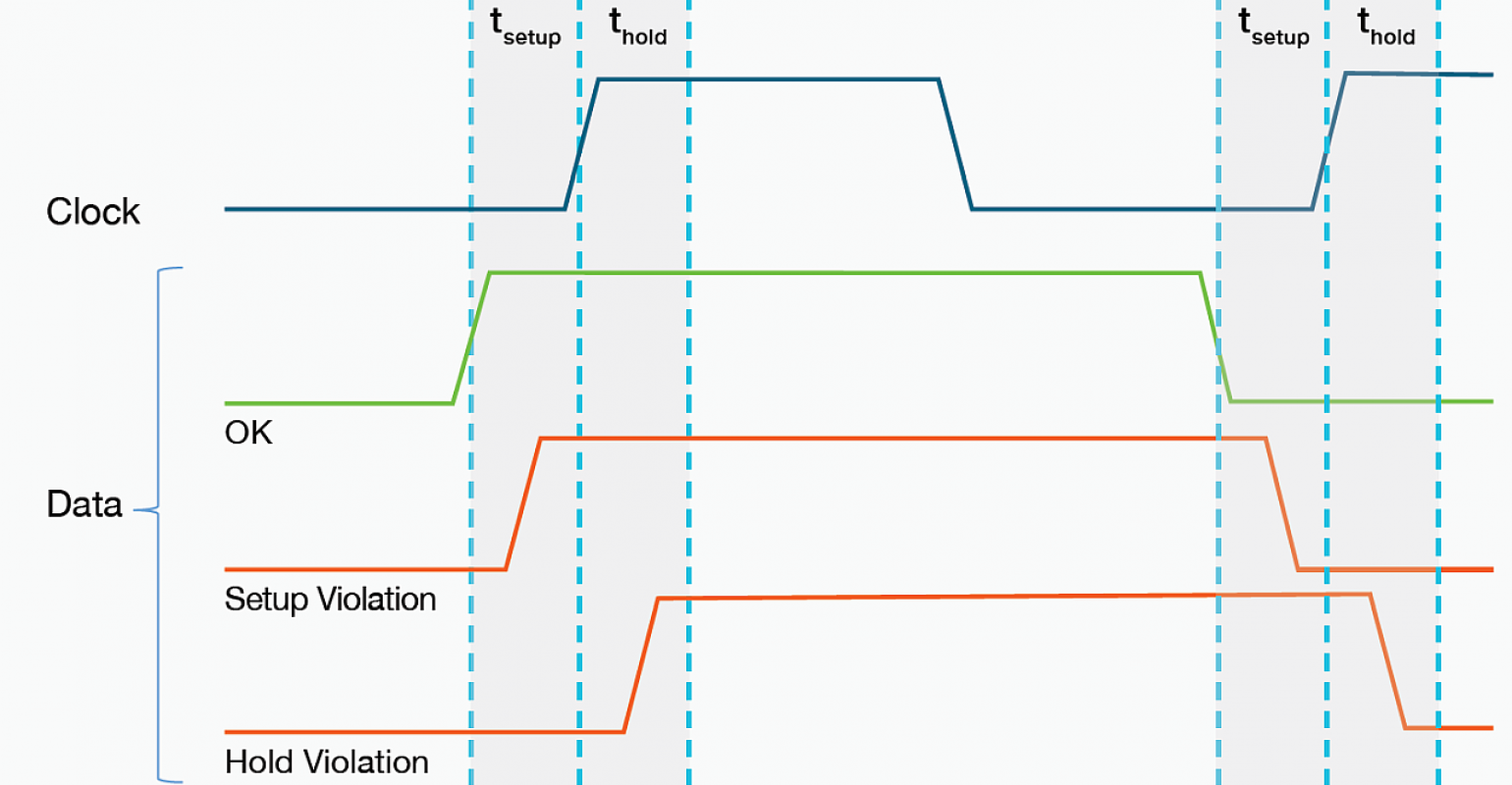 Image from Design News
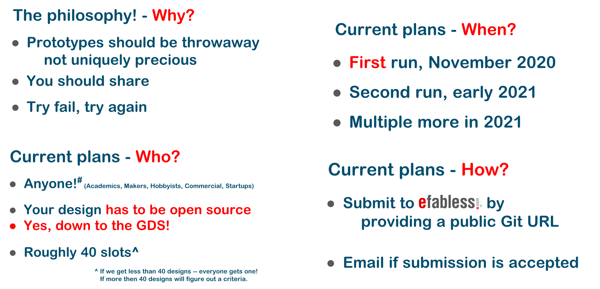 Image from Tim ‘mithro’ Ansell’s FOSSi presentation
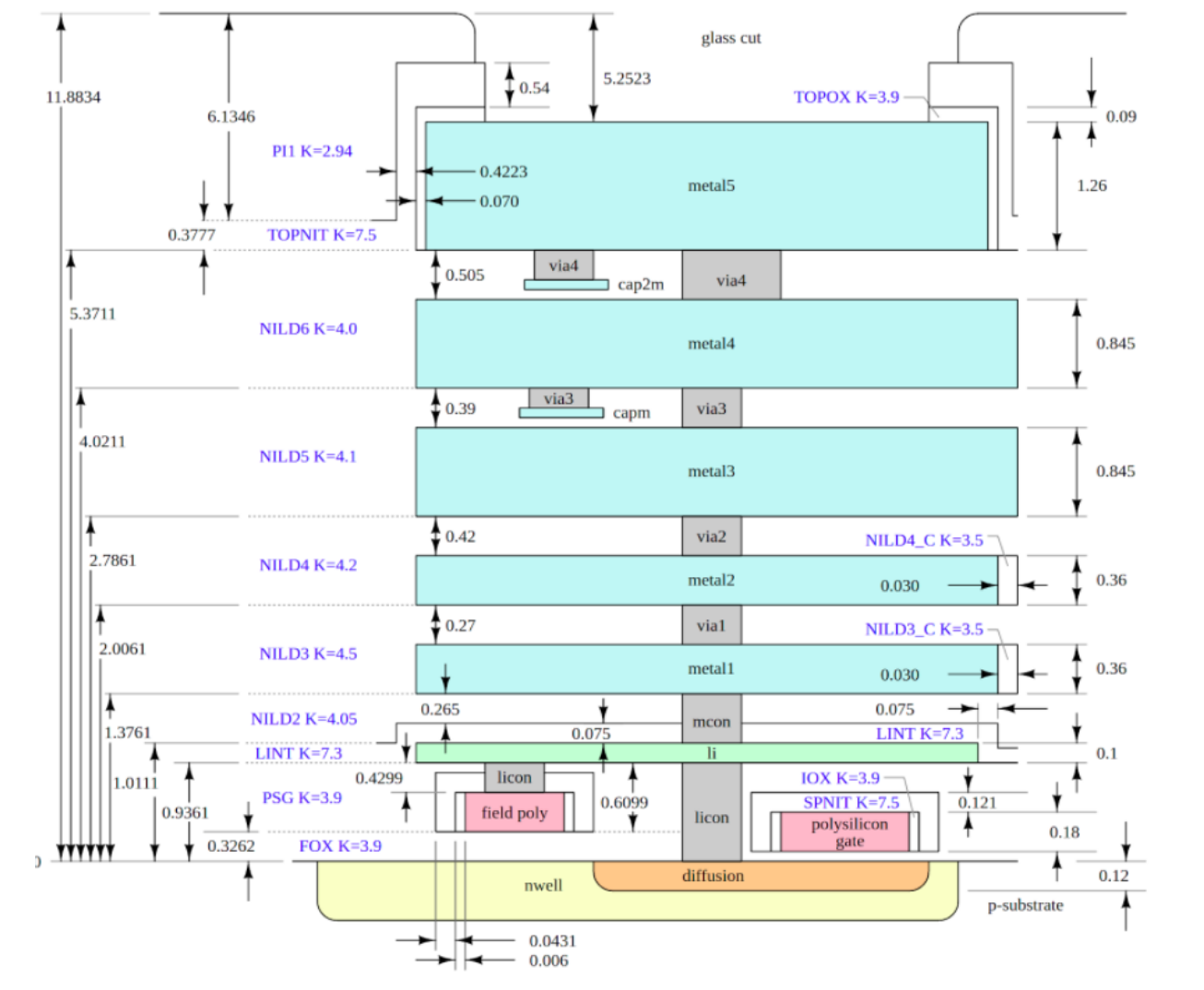 Image from Skywater PDK docs
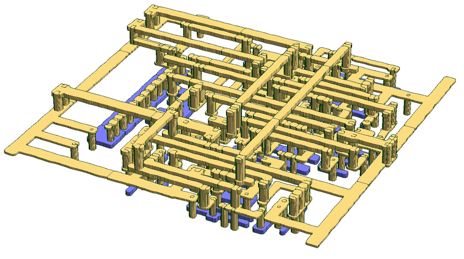 Image from Wikipedia
 Image from SCU digital collection
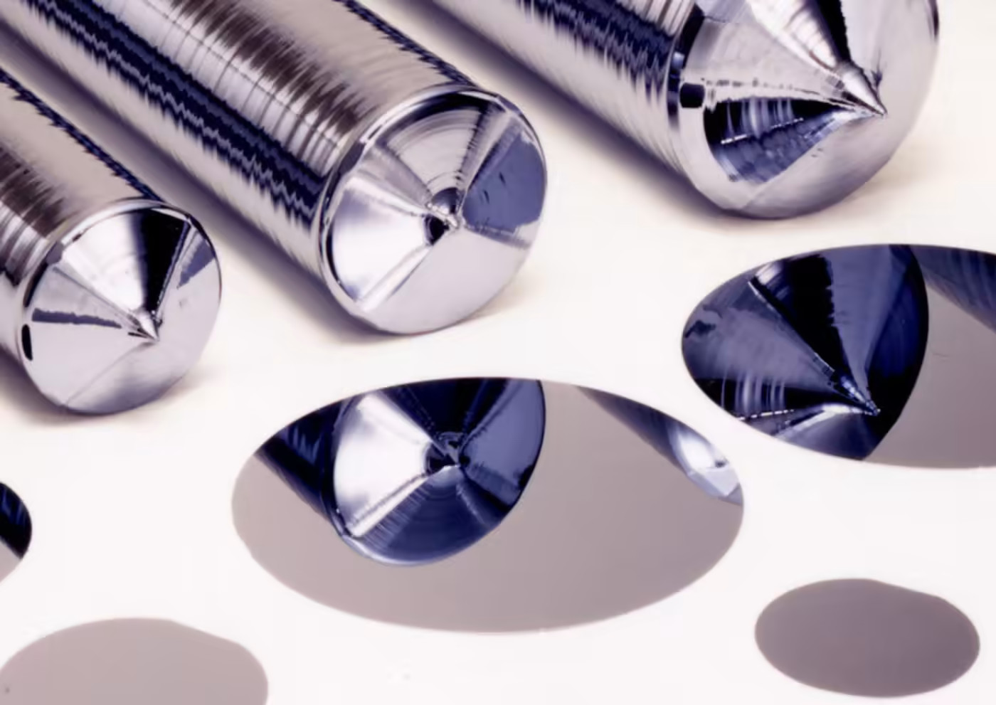 Image from Nikkei Asia
Image from Wikipedia
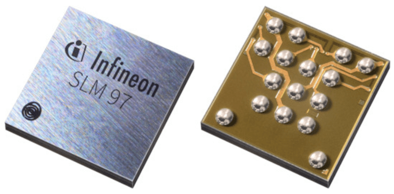 Image from EET Asia
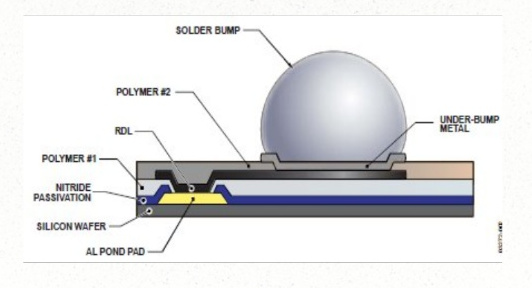 Image from