Short articles about my experience with making ASICs, interviews and any other related topics I think are interesting.
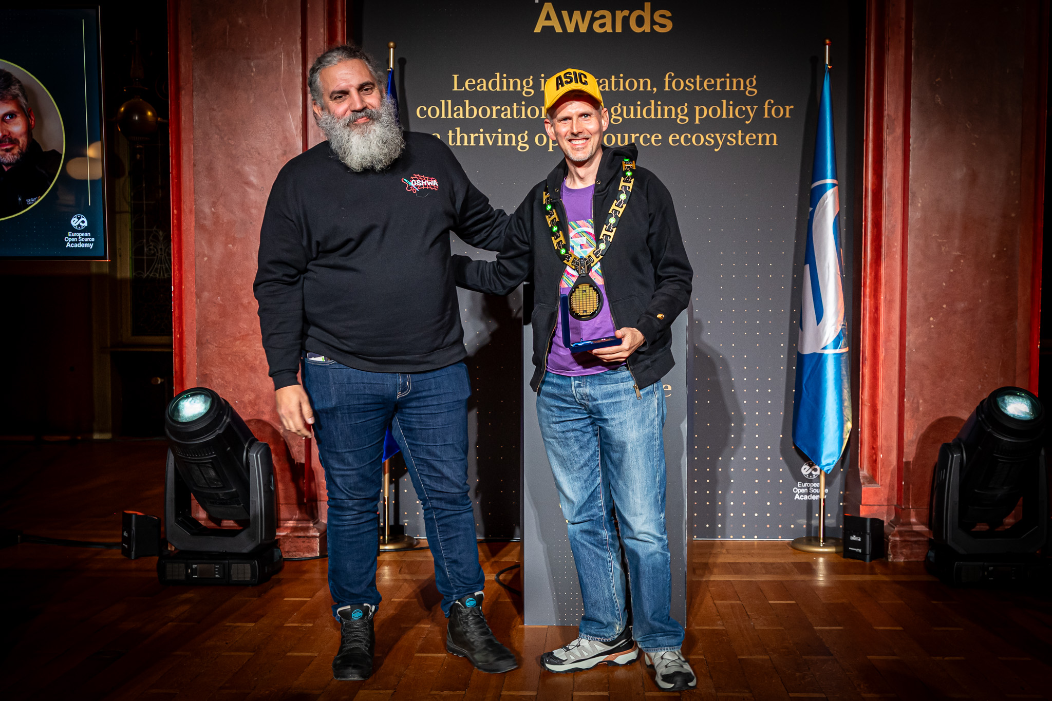
EOSA award for Skills and Education
Review of 2025 and goals for 2026

For the first time, open silicon wasn’t just a niche experiment in 2025 - it was a real ecosystem spanning three fabs and thousands of designs. And then one company collapsed and hundreds of chips effectively disappeared overnight.
Efabless going out of business at the end of February hit the community like a hammer. They weren’t just an MPW provider - they offered hundreds of packaged parts with no NDAs, great pricing, and a level of openness that was rare in silicon. Losing them left hundreds of designs, including 500 Tiny Tapeout projects from TT08 and TT09, seemingly stuck in fabrication limbo.
Test Equipment Grant 2025
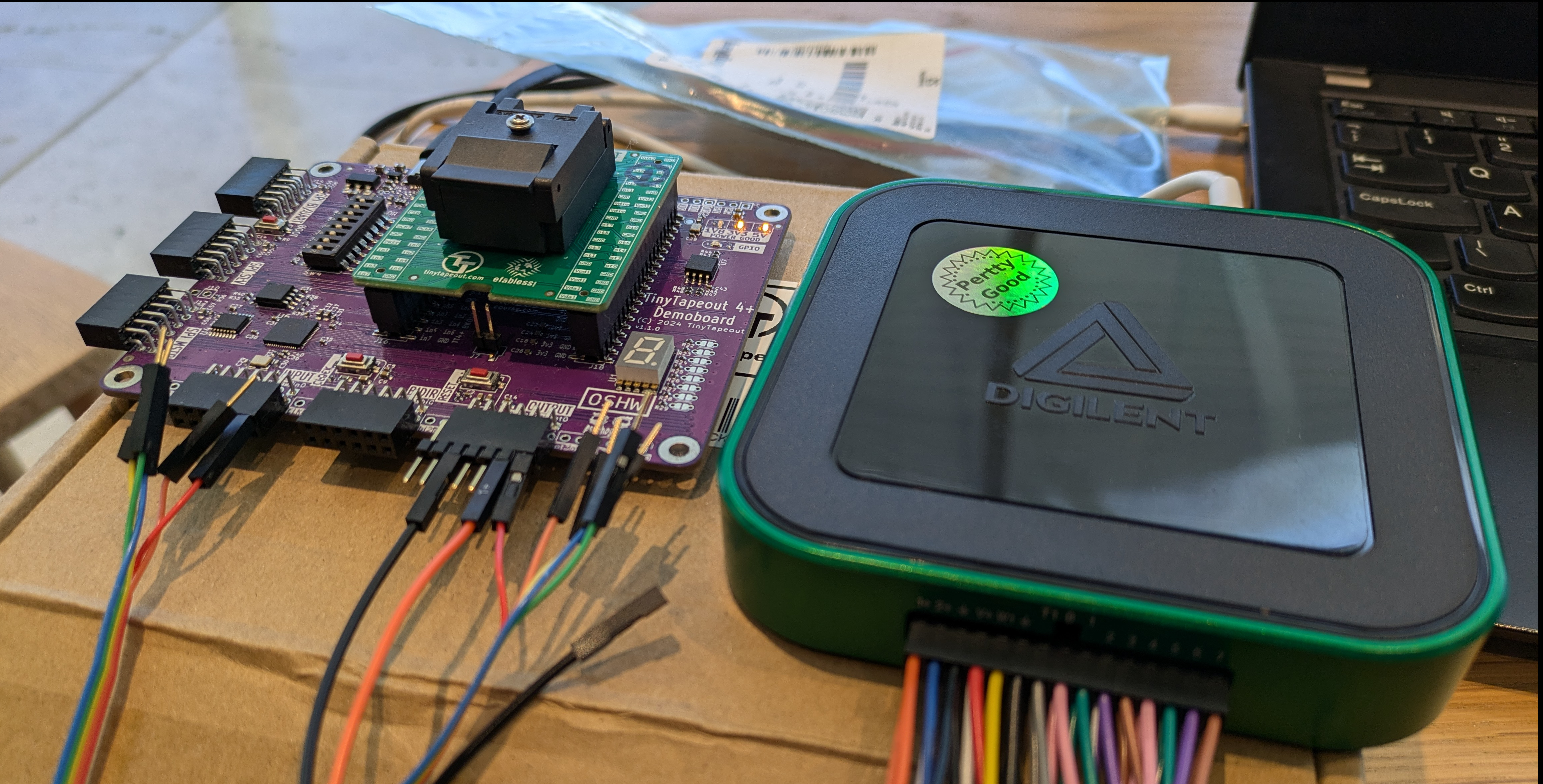
Applications for the grant are now closed.
It’s become a cliche, but hardware is hard!
One reason why hardware is harder than software is that the time between revisions is often longer. We need to wait for new PCBs, or for components to be delivered. Or for more new PCBs after we realise we got it wrong!
Another reason is that it can be expensive, and not just for the physical components. We generally need more of a lab than software developers. Not just soldering irons and good lighting. Test gear is essential for learning how your circuit is actually behaving, matching simulation to the real world. And it’s usually expensive.
Excited by silicon!
I was recently asked what excites me most about the exploding open-source silicon ecosystem. Honestly? It depends who’s asking.
For one person I might talk about Basilisk - the PULP team’s seriously impressive Linux-capable RISC-V core. For another, maybe the new GF180mcu MPW from Wafer.Space, or the millions in funding finally flowing into improving the tools. And then there are the community events that make the whole thing feel electric.
There’s a lot happening at once, so to make sense of it, let me break it down into Foundries, Funding, Tools, IP, Community and the Future.
Celebrating 20k YouTube Subscribers

Since I started my channel in December 2020, I’ve posted 181 videos that have been watched 660k times for a total of 35k hours! To celebrate reaching 20k subscribers I wanted to share some of the ones I’m especially proud of, and why they matter to me.
I’d say my all time favourite was when I used a particle accelerator to look inside my own microchips!
I met Tomas Aidukas at the Free Silicon Conference. In his talk, he showed an amazing 3D view inside a microchip - captured using a technique called ptychographic X-ray computed tomography. I asked if he’d be interested in imaging one of my open source chips. It turned out that having the source files for the chip was actually pretty unique.
Testing projects with GitHub actions

For the past two years, I’ve used GitHub Actions to automatically test the install instructions for the Zero to ASIC course. Now, as I work on a major update, I’m taking it further: I’m adding CI tests for every one of the 10 practical projects.
The goal? Make sure students never run into out-of-date instructions or broken software.
To do this, I’ve been exploring Harald’s IIC-OSIC-TOOLs Docker image and built a new composite GitHub Action.
Sky130 Inverter Instructions

Review of 2024 and aims for 2025
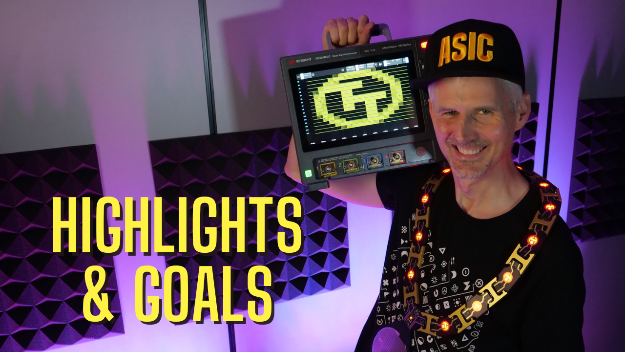
Wow what a year! In this post I’m going to look back over 2024 and share some of my highlights and the goals I met and failed. Then I’ll share my ambitions and predictions for 2025.
With all the open source tapeouts, events, workshops and news, there’s a ton to cover - so let’s jump in!
I aimed for 2000 new people to get started with open source silicon via my courses and tiny tapeout.
Test Equipment Grant

Applications for the grant are now closed.
It’s become a cliche, but hardware is hard! One reason why hardware is harder than software is that the time between revisions is often longer. We need to wait for new PCBs, or for components to be delivered. Or for more new PCBs after we realise we got it wrong!
Another reason is that it can be expensive, and not just for the physical components. We generally need more of a lab than software developers. Not just soldering irons and good lighting. Test gear is essential for learning how your circuit is actually behaving, matching simulation to the real world. And it’s usually expensive.
Chip On Board
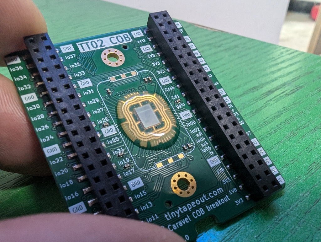
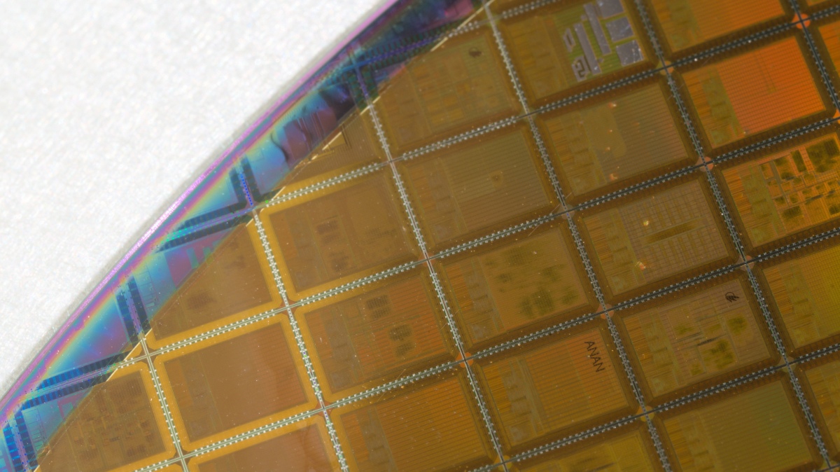
Our first COB (chip on board) chips are working! This has been a dream of mine for a few years, and it’s finally a reality!
We’re used to seeing chips as little black boxes on a circuit board, but what’s inside?
The first part of the journey started with Tamas creating this cool circuit board.