Short articles about my experience with making ASICs, interviews and any other related topics I think are interesting.
VGA clock
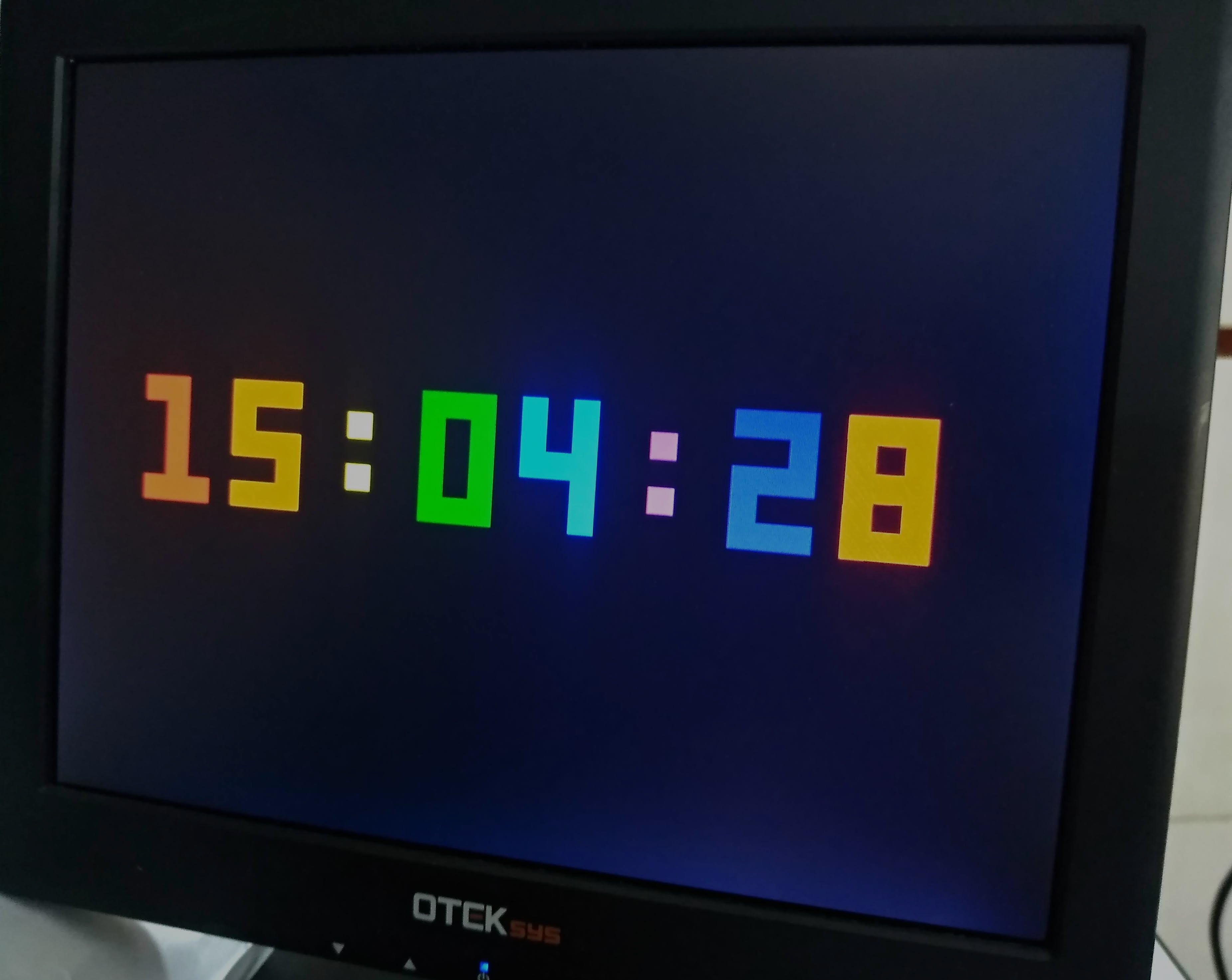
This is one of the first projects I hardened using OpenLane.
News update: my clock works! And you can buy a kit here!
Still can't quite believe I have a clock on my desk that is powered by a chip I designed! pic.twitter.com/O5c2omQYYp
— Matthew Venn (@matthewvenn) March 31, 2022
It shows the time on an LCD panel. It will be part of my first tapeout.
After running the OpenLane ASIC flow, it results in a design that uses 180x180 microns (32000 square microns). As we have about 10e6 square microns in the user project area of the Google shuttle, I could potentially put about 300 of these on the ASIC!
Multi Project Harness
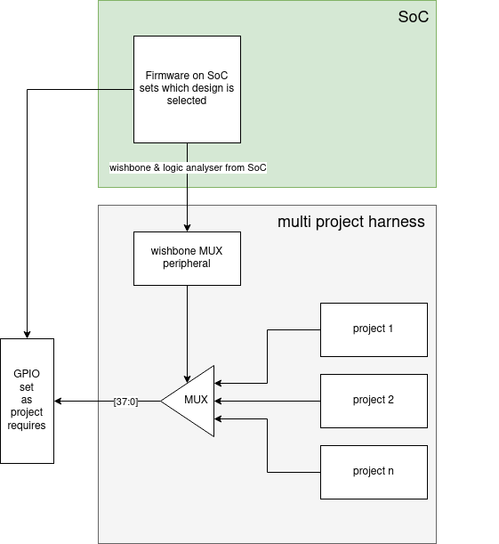
The Google/Skywater Shuttle has about 10 square mm of space for your project. This sounds tiny but is actually HUGE for many beginner projects. Read this post to find out what you could fit in the user space.
For the Zero to ASIC course, I want to aggregate all your designs together into that area, so we need to do some extra bits:
- Multiplex all the inputs and outputs of your project to the GPIO pins of the Caravel harness.
- Connect important signals like clocks and make sure the tools know they are special
- there will need to be a bit of firmware on the SoC that sets up the GPIOs for each design and sets it active.

Inverter
A standard cell is a building block that contains some basic digital or analogue functionality. These blocks are then tiled together to make the final design.
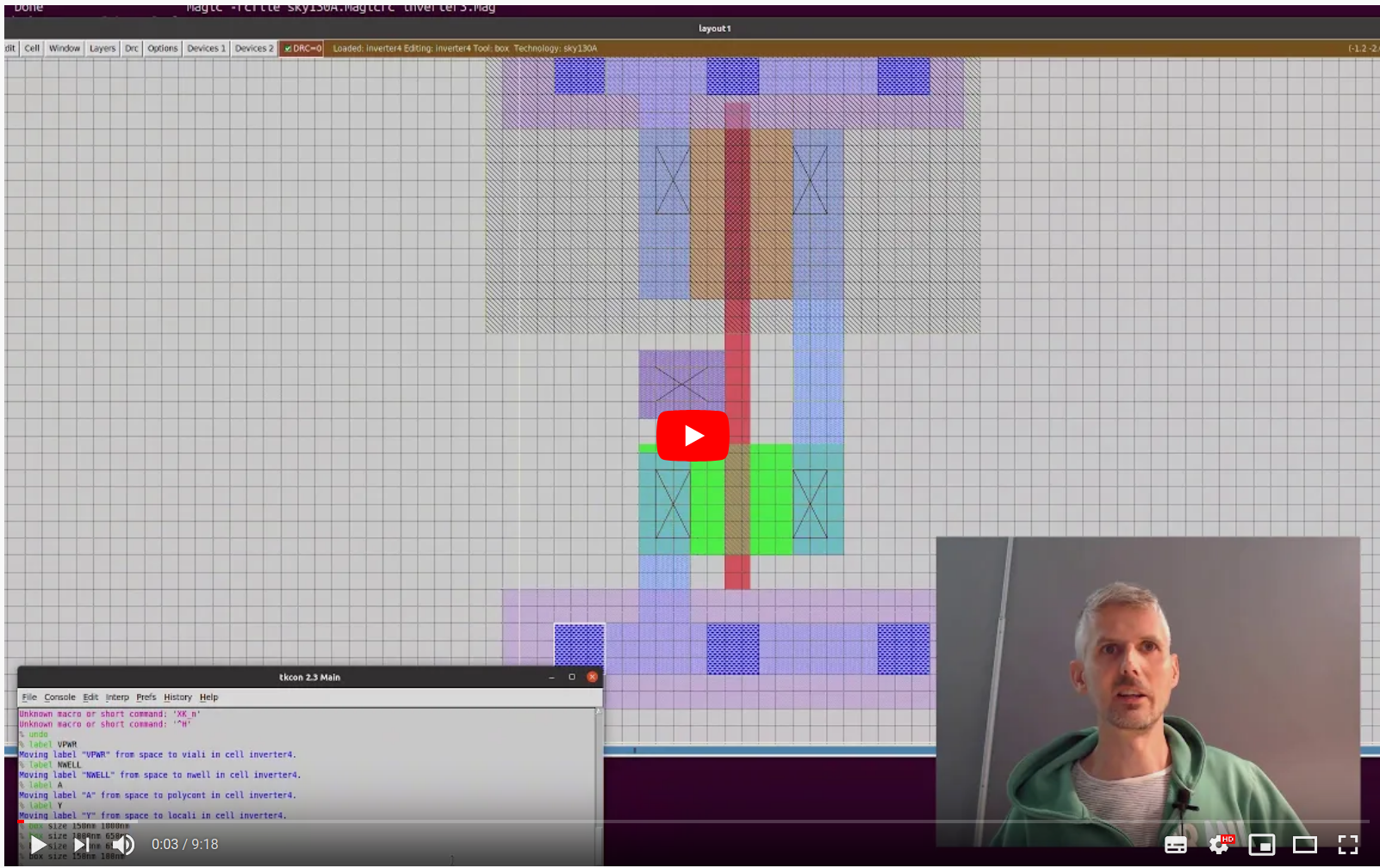
Since finding out about the Skywater PDK, I wanted to try drawing my own ‘standard cell’ using the Skywater transistor models.
An inverter is one of the simplest and even that was quite difficult! As you can see below it contains an N and P type MOSFET.