PDK
The Process Design Kit is a library of all the specifications that describe a particular factories’ particular chip fabrication process. This often includes representations of the design rules and devices which can be used by particular implementation and verification tools that have been checked and approved by the fab. This may include software representations of items such as transistors which will be automatically laid out with the dimensions that meet the rules for the process (often called pcells for ‘parameterized cells’ - the designer says what size is wanted, the pcell does the rest).
In our case we have access to the Skywater factories 130 nanometer process, usually called sky130.
Tim Edwards:
Note that this process is advertised as a “hybrid 180nm / 130nm”.
A number of aspects are either very close to a 180nm process or somewhere between 180 and 130.
The typical minimum length low-voltage transistor is 150nm.
For more information about process sizes see this about the node.
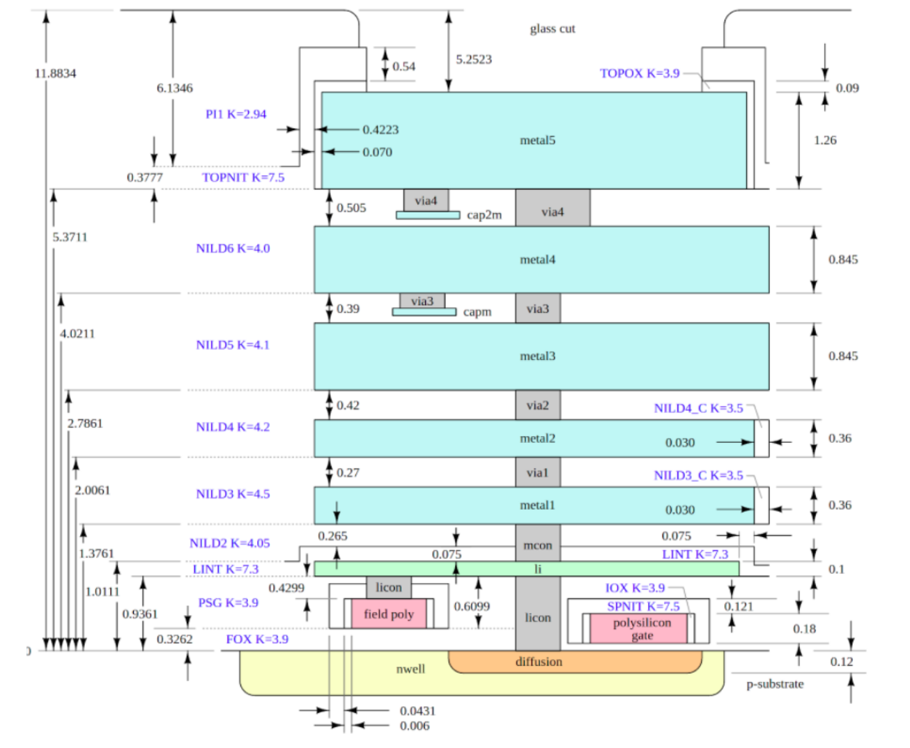
This picture shows how the layers of the chip stack up to form the complete ASIC.
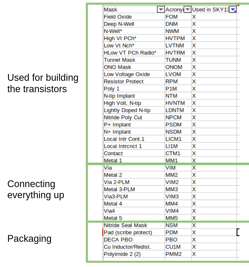
This table shows all the layers defined in the PDK that can be used in a design tool like Magic.
For the raw data, check the mask definitions
You can get all the information here: https://skywater-pdk.readthedocs.io/en/main
The following is adapted from one of Tim Ansell’s slides in his Fossi presentation
Design Rules
Behavioural models
This allows us to model analog and digital components, for example different sizes of MOSFET.
Support IP
- Input Output libraries
Analog design
- Spice models
Digital design
- Standard cells
- Timing models - allow us to know how fast we can run our designs
Course feedback
I think that starting from zero you will learn enough Verilog to write something that synthesizes and runs and then they you can harden into a design and that would be a pretty rad intro to to Verilog.
Zbychu (digital course)