Shuttle
A shuttle service is the same as a multi project wafer.
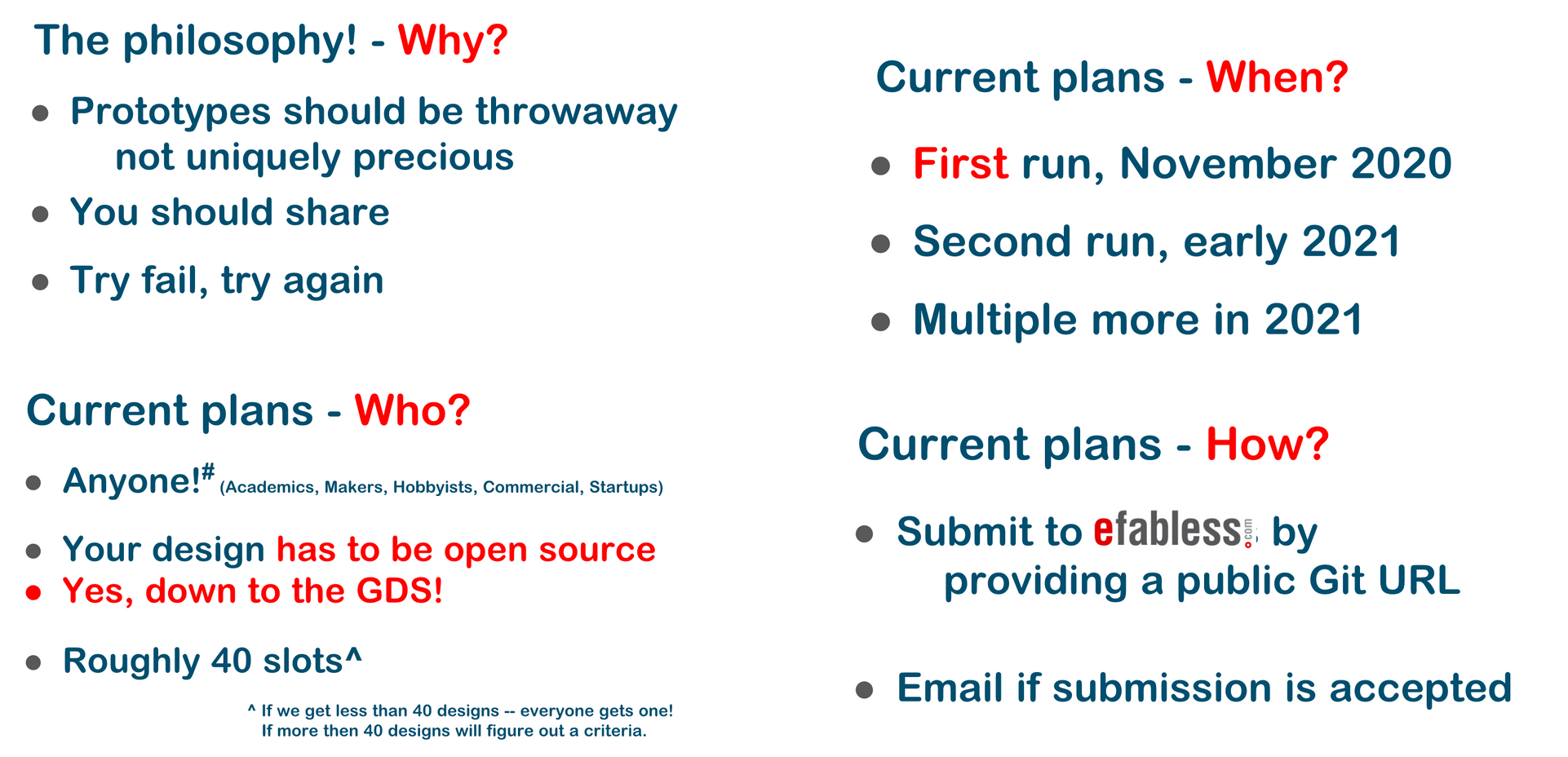
On 30th June 2020, Tim Ansell announced the collaboration between Google and Skywater to provide a free shuttle service in his FOSSI dialup talk.
These slides taken from his talk show the overview:
Chip Foundry Shuttle
Normally in an MPW you would have the whole die to yourself. In the ChipFoundry Shuttle all the designs will be within the user project area of the Caravel harness.
Caravel has its own RISCV processor and a neat datasheet. The idea here is to make it easier to bring up and debug your designs at the cost of some area.
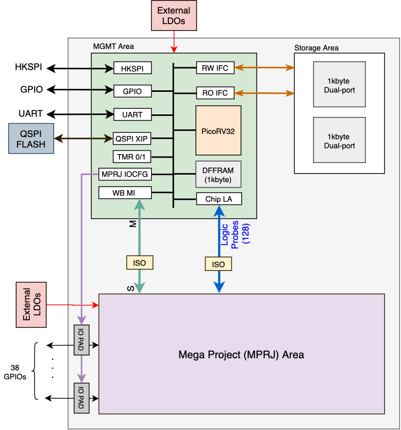
Read this post to find out what you could fit in the user space.
The Google shuttle returned chips in type of packaging called Wafer Level Chip Scale Packaging and then the easier to handle QFN.
Course feedback
After submitting a digital project for Tiny Tapeout 2, I wanted to up the complexity level and do something analog. The analog course gave me the knowledge and tools to do so. It is perhaps the only place that can get you from 0 to a working analog design ready for tapeout in a matter of weeks.
Michael Bikovitsky (analog course)