MPW
A Multi Project Wafer is used to reduce the cost of making an ASIC. By using a lot of different designs on the same wafer the Non Recurring Engineering (NRE) costs of making the mask set are shared between all the participants.
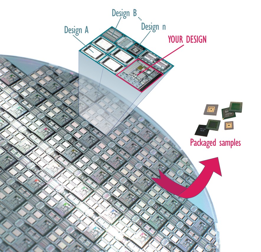
The Google shuttle is an example of an MPW.
Our MPW submissions
So far we have made 4 tapeouts to the Google MPWs:
MPW physical implementation
We sent John McMaster some chips to take a look at from MPW1. Here presented his findings at OpenTapeOut
And you can browse his microphotographed die here
Course feedback
If you've got any interest in how the sausage is made you should get on the course and you should dig in and find out more. I mean this was the work of secret witches and wizards in mysterious cloaks casting strange incantations over a cauldron! This was all secret stuff and I love that this project is trying to do to silicon design what the open source community has been trying to do with software for the last 30 years. This feels like the next logical step and I think we'll look back and say well of course you can make your own chips that's just a thing and it will just be obvious and commonplace and I look forward to that.
Jonathan Pallant (digital course)