Short articles about my experience with making ASICs, interviews and any other related topics I think are interesting.
MPW2 announced by Efabless

Efabless have announced MPW2! The closing date is the 18th of June.
The biggest changes are:
- OpenLANE ASIC flow updated to rc0.15
- Caravel has become caravel_user_project at the mpw-two-c tag:
- smaller repo size includes a ‘Caravel Lite’ submodule
- new IRQ ports
- logic analyser registers renamed
- An alternative analogue specific ‘Caravan’ harness
- The submission process has been streamlined to make it faster and easier to submit
You can browse the current applications here: https://platform.efabless.com/projects/shuttle_name/MPW-2
Interview With Dan Rodrigues - first shuttle, racing the beam & retro gaming

In this interview Dan and I talk about his submission to the first shuttle, simulating video projects, how to do graphics with no frame buffer and the joys of retro gaming.
- Caravel repo: https://github.com/dan-rodrigues/caravel_vdp_lite
- IceStation32: https://github.com/dan-rodrigues/icestation-32
LibreLane Output Files
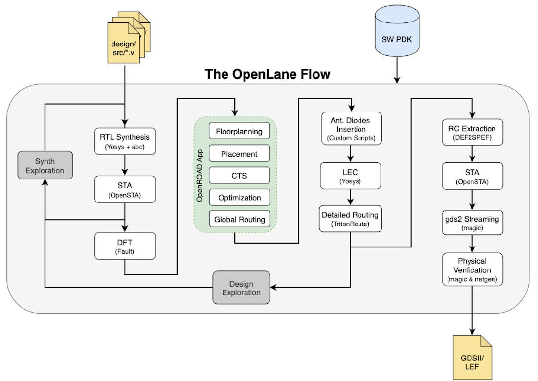
LibreLane makes a lot of output files! This can be quite confusing when you’re getting started.
Here’s a useful spreadsheet I made to show:
- the path of the files
- most important files and what they mean
- which tool creates which file
Thanks Amr and Ahmed for helping me with this!
The spreadsheet was updated for LibreLane in 2025.
LibreLane summary tool
I’ve also made a summary tool: https://github.com/mattvenn/librelane_summary
This allows you to easily:
Interview With Thomas Parry - Amateur satellite radio, Open Source vs Industry tools and beautiful analogue layout
In this interview Thomas talks us through his Amateur satellite transceiver shuttle submission. We also discuss the differences between the Open Source tools and the industry standard ones he uses in his day job.
- Design repo: https://github.com/yrrapt/amsat_txrx_ic
- Caravel repo: https://github.com/yrrapt/caravel_amsat_txrx_ic
- Connect with Thomas on linkedin: https://www.linkedin.com/in/thomas-parry-60419468/
My Zero to ASIC journey
Almost exactly a year ago in March 2020 I started getting interested in Open Source ASIC tooling. I don’t remember exactly what sparked my interest, but I remember this talk by Tim Edwards at WOSH: Bootstrapping a real working design flow and sometime after seeing Adam Zeloof posting a picture of an ASIC implementation of pong.
I began by investigating QFlow. The standard cells used by QFlow were from Oklahoma State University (OSU).
By May I was getting a few results out of QFlow and I was curious to discover how digital logic actually works on silicon. I experimented with Magic and managed to draw and simulate an inverter after taking one of Kunal Ghosh’s VLSI courses.
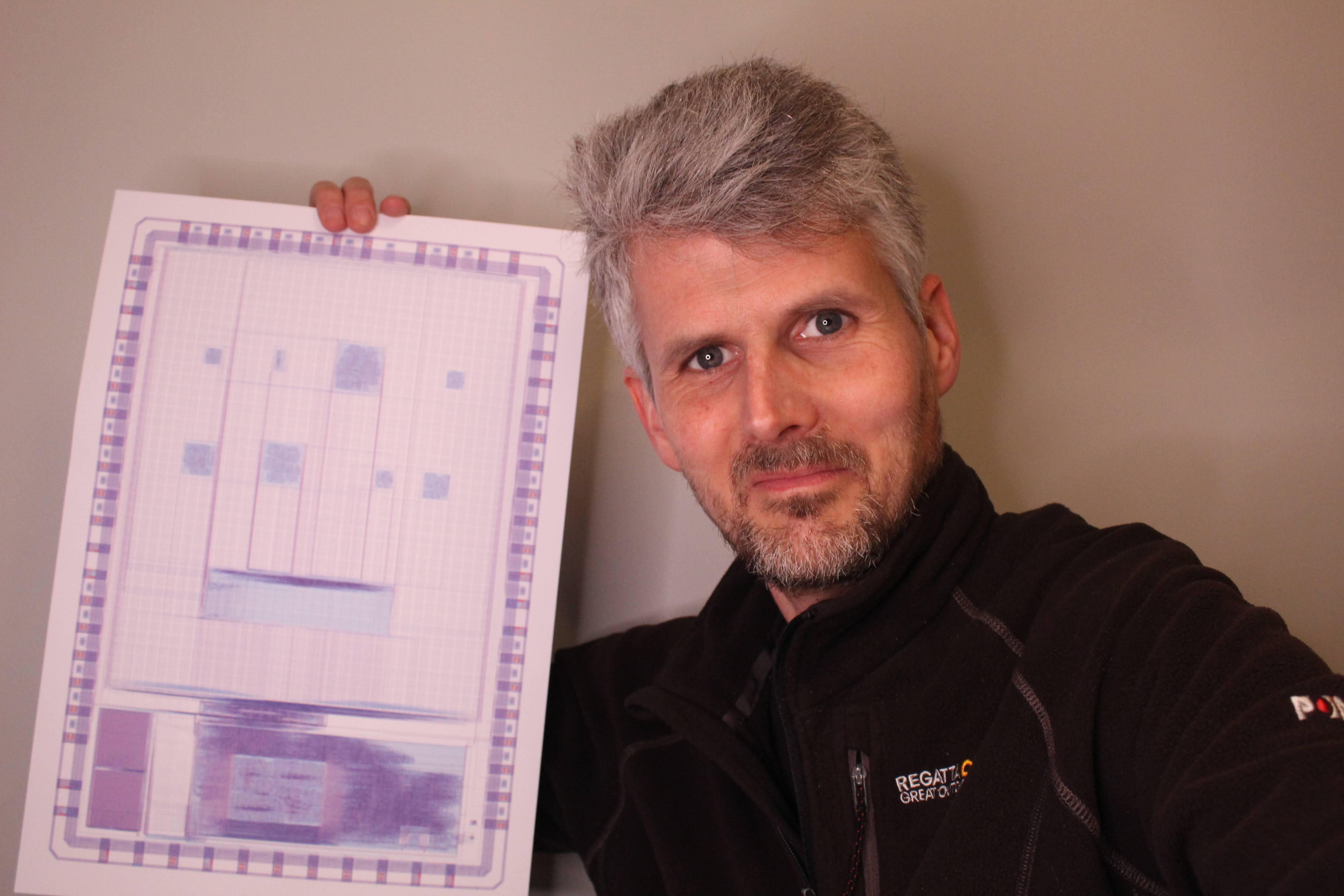
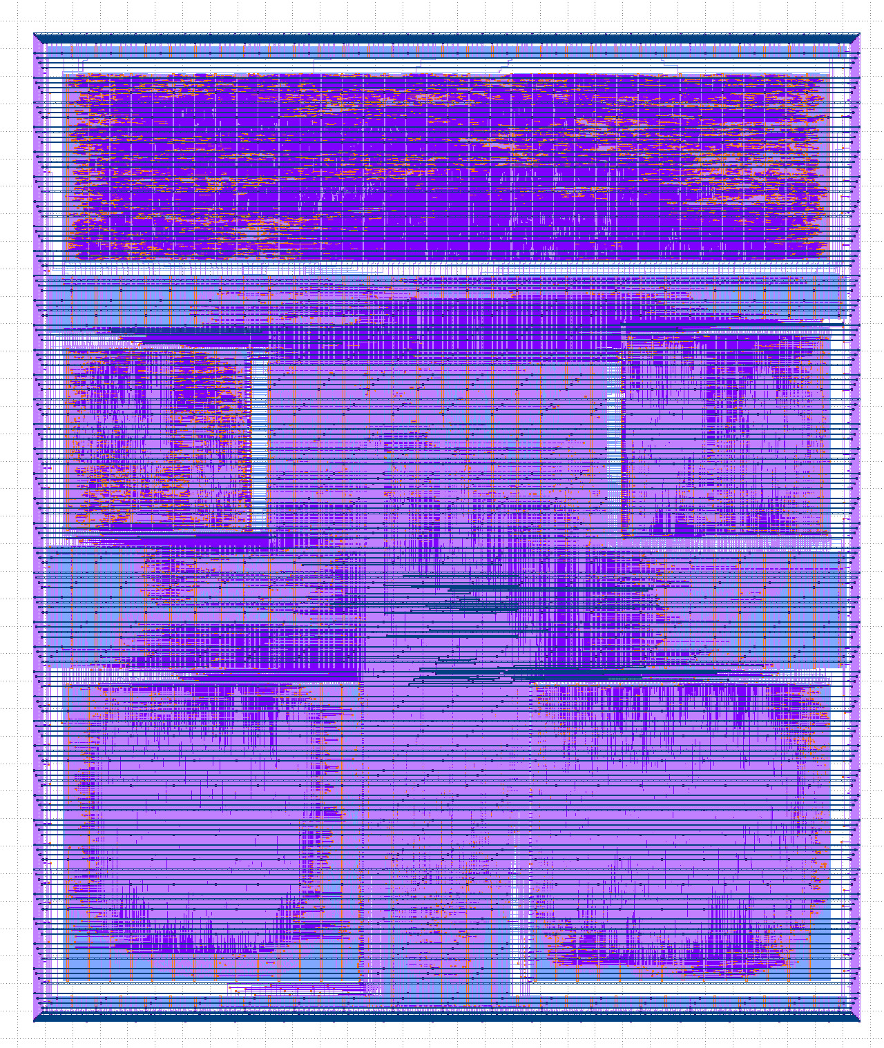
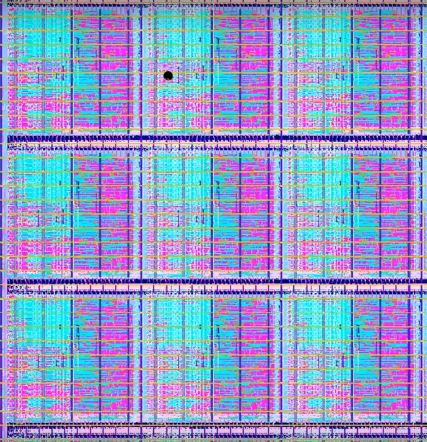
Printing my first ASIC's GDS files
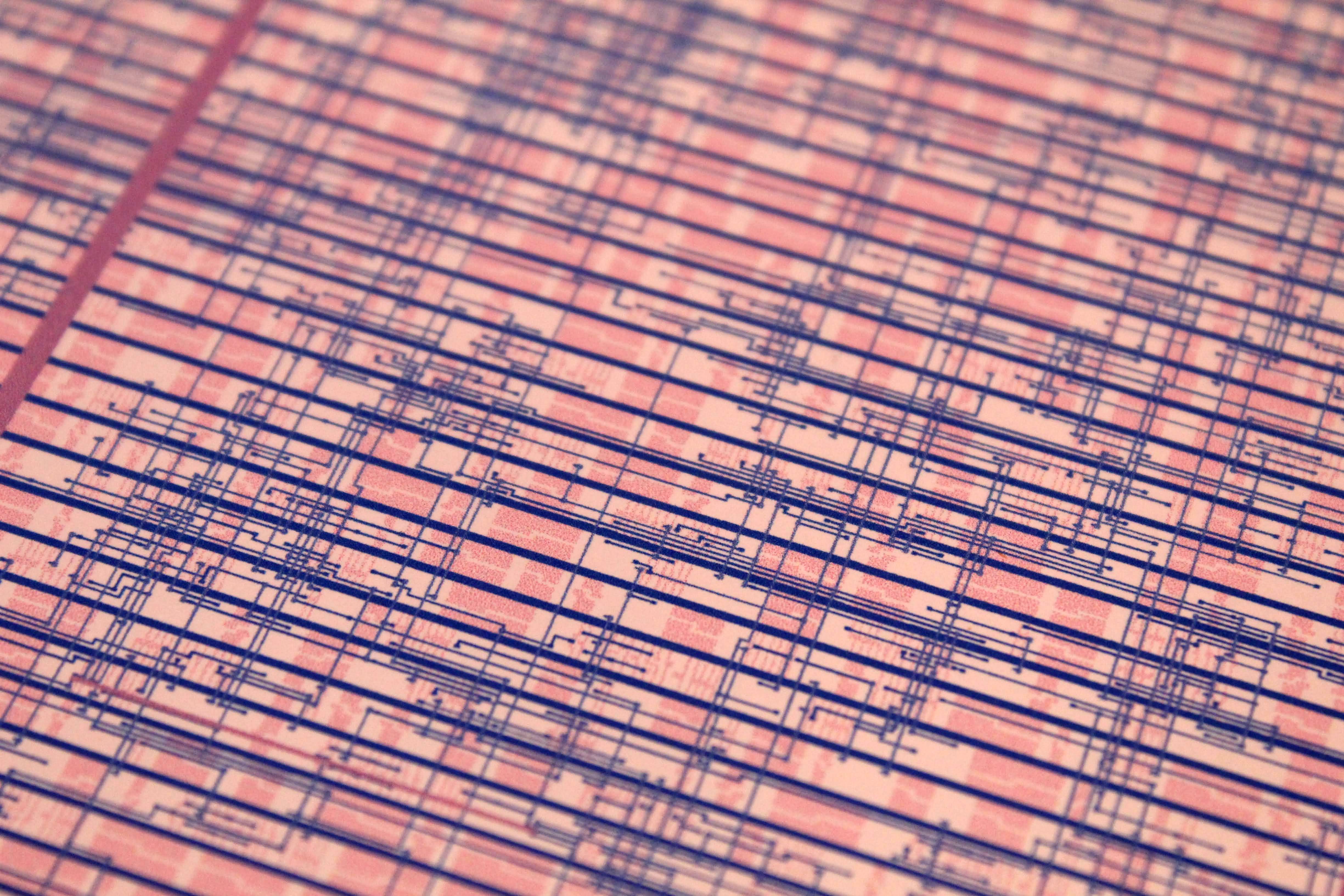
I’ve been wanting to try plotting or printing the GDS files from my first ASIC for a while, and finally I’ve had some time to have a play. I used KLayout because it’s easy to change colours, show and hide layers, and export to a high resolution PNG.
I want to make a poster with 3 pictures inside:
- The whole chip,
- Zoomed into the VGA clock macro,
- Zoomed into the standard cells.
Here’s a photo of the print (I know, how meta) of 1:
Understanding Caravel GPIO
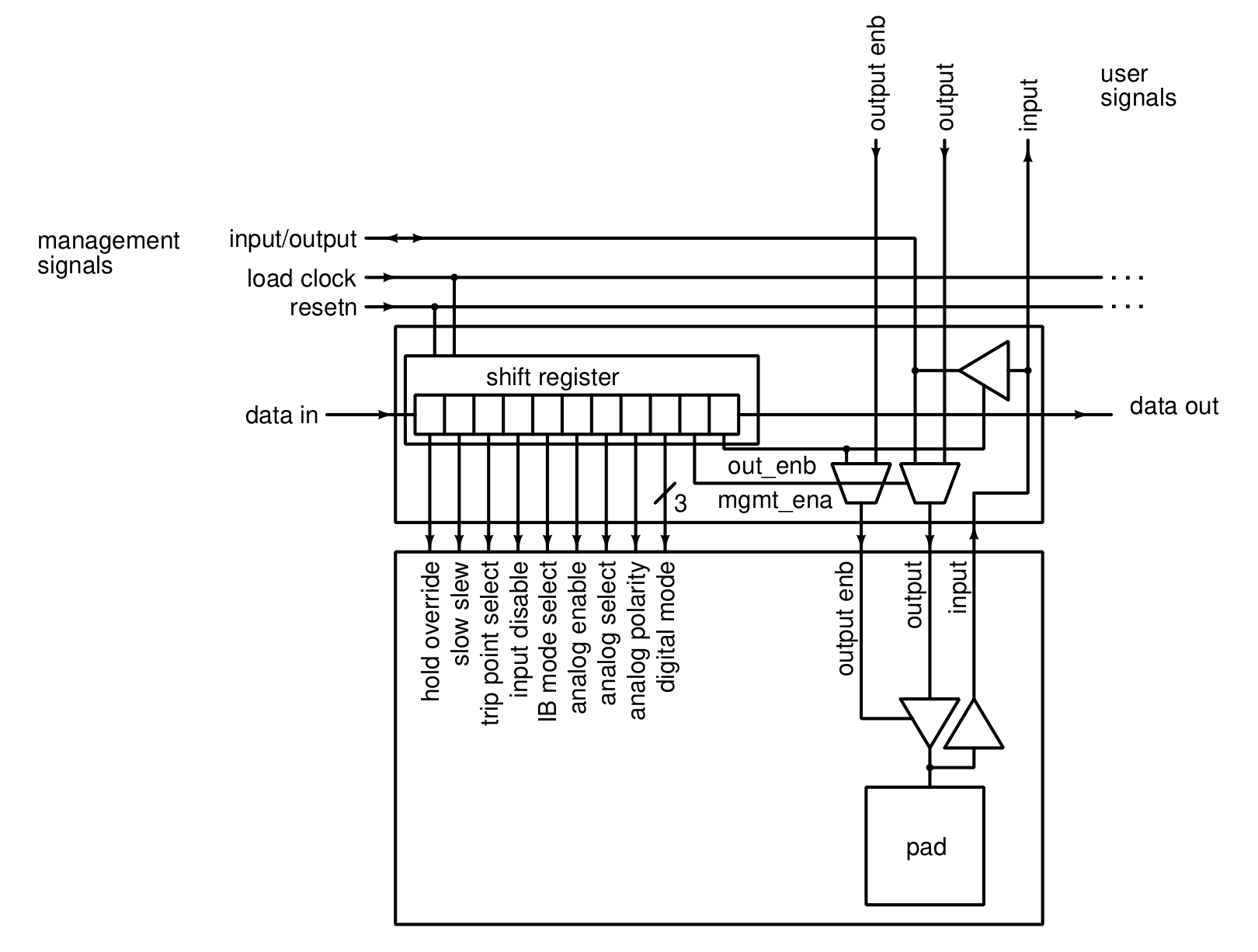
When I was first testing my designs inside Caravel, I was quite confused about all the GPIO options.
- Each pin has a range of options that can be configured by firmware running on the RISCV processor.
- Each pin can be driven from the processor or your custom design.
- The outputs have separate output enable lines for bi-directional signalling.
I put together an experiment where I tried the most important options and checked the results in a simulation. You can watch the video here:
Interview With Anton Blanchard - Microwatt: a 64 bit OpenPOWER core, VHDL and OpenLane
I interviewed Anton Blanchard about his MPW1 application - a 64bit OpenPOWER core written in VHDL.
We talked about:
- VHDL vs Verilog
- FPGA vs ASIC
- Problems they faced with such a big design
- SRAM vs DFFRAM
- Software vs Hardware mentality
- Fixing bugs and contributing to OpenLane
You can check out the repository here: https://github.com/antonblanchard/microwatt-caravel
Last minute DRC fixes
The story of the first Open Source ASIC shuttle continues!
A few of the applicants to the first shuttle were recently contacted by efabless - they had discovered some DRC issues that couldn’t be waived by the foundry.
In my recent interview with Tim Edwards, he mentioned that Google are paying for a license of Calibre - another swiss army ASIC tool like Magic. This is to help make sure that the OpenLANE DRC hasn’t missed anything.
Interview with Tim Edwards - what happens between ASIC submission and sending to Skywater?
In this interview I talk with Tim Edwards from eFabless. He is their vice president of analog and platform.
We mostly talked about what needs to happen before they send the final files to Skywater.
A lot of the work is infrastructure:
- fetching files,
- compositing IDs,
- generating fill layers,
- a final DRC run.