World's first certified open source hardware down to the chip level?
I’m very pleased to get OSHWA certification for my ASIC clock. I’m pretty sure this is the world’s first certified open source hardware down to the chip level!
Update! The PCB has been updated here.
The clock was submitted as part of MPW1. We’re expecting silicon back in August/September, so it was time to get the PCB ready and try to source the other components!
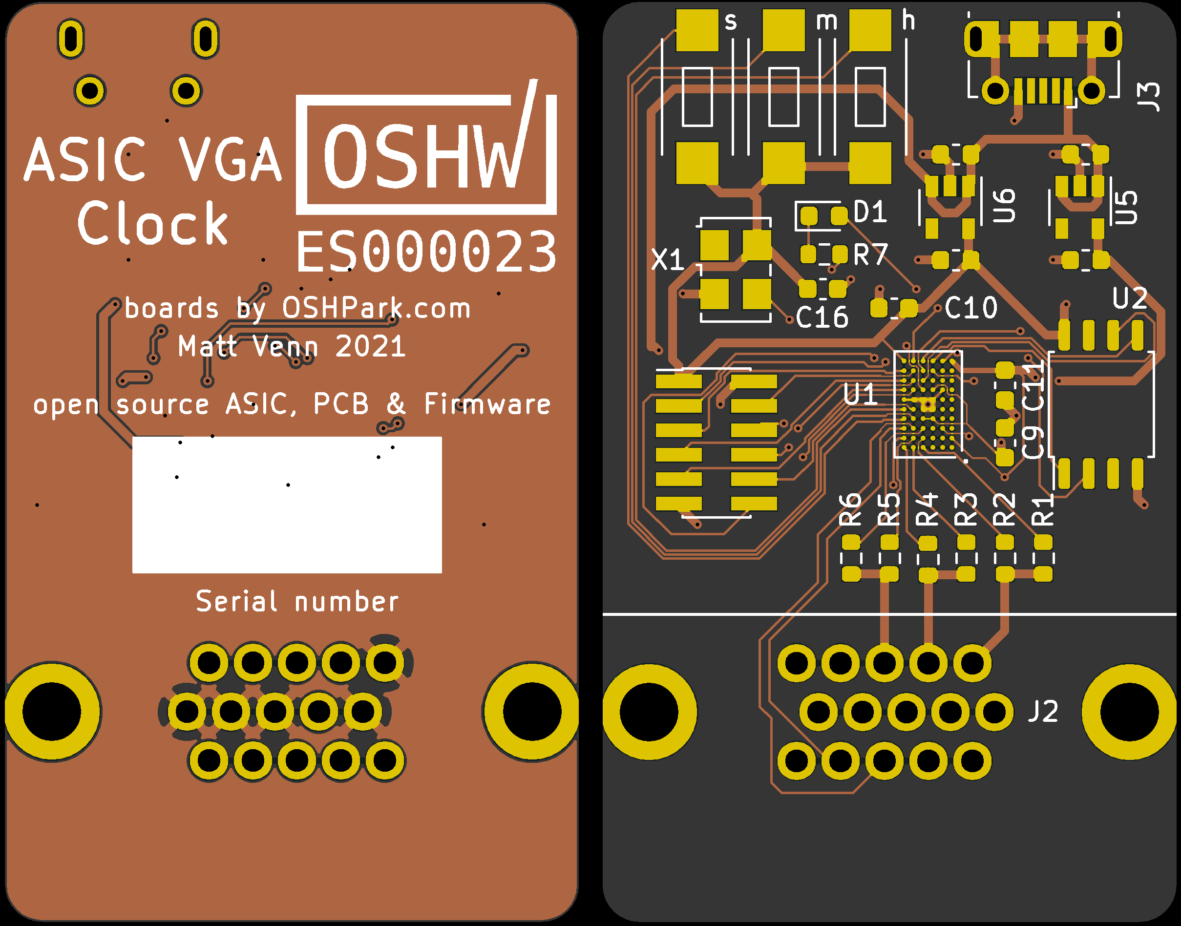
I started off by forking Sam Littlewood’s carrier board. This is a 4 layer board, but as I don’t need all the signals I was able to get it down to 2 layers for cheaper fabrication. OSHPark have sponsored the board in their special ‘after dark’ finish.

As well as the ASIC and the VGA socket, we also need:
- voltage regulators for core and IO
- flash memory for the firmware
- an oscillator
Why do we need flash for firmware? It’s because Caravel, the ASIC harness uses a small RISCV processor to assist with bringup. Part of its job is setting up IO, for example whether pins are inputs or outputs. It also configures the internal PLL so we can get an internal clock frequency that matches the VGA frequency (31.5MHz).
The PCB was designed in Kicad and you can get all the files here: https://github.com/mattvenn/vga_clock_pcb
The ASIC pinout was thoughtfully done by Tim Edwards at Efabless. We can escape all the signals we need without a 4 layer board (for this case), and the collection of ground pins in the middle means we can use a via there to get all the grounds out at once.

I plan to put a few of the finished boards up on Tindie as a collectors item, and donate the proceeds to OSHWA.