CMOS
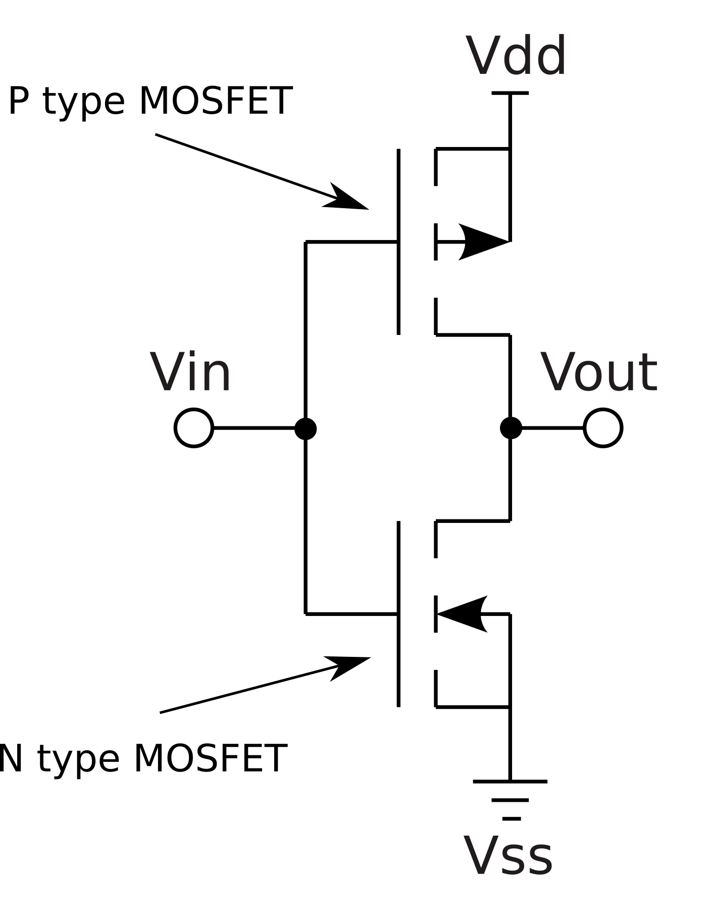
CMOS was introduced to ICs in the late 1960s. P type MOSFETs are used to pull output signals up, and N type MOSFETs are used to pull output signals down - P and N are the complementary types.
Before CMOS, NMOS was used for digital logic. NMOS isn’t very energy efficient because the pullup is performed by a resistor which is dissipates energy when the N type transistor is pulling down. It also is hard to balance the pullup and pulldown speeds which makes design difficult.
By using transistors for both pullup and pulldown we get better energy efficiency. When the inputs are stable, only one transistor is on at a time so there is no static current consumption, but during input switching a small amount of current may flow directly through the P then through the N transistor: this is called crowbar current. Normally the transistors are designed to avoid or minimise this unncessary power consumption.
https://en.wikipedia.org/wiki/CMOS:
Complementary Metal Oxide Semiconductor (CMOS) is a type of MOSFET fabrication process that uses complementary pairs of p-type and n-type MOSFETs to build logic functions.
Here is a CMOS inverter showing the complementary N and P type MOSFETs.
And here’s how it could be laid out using a tool like Magic
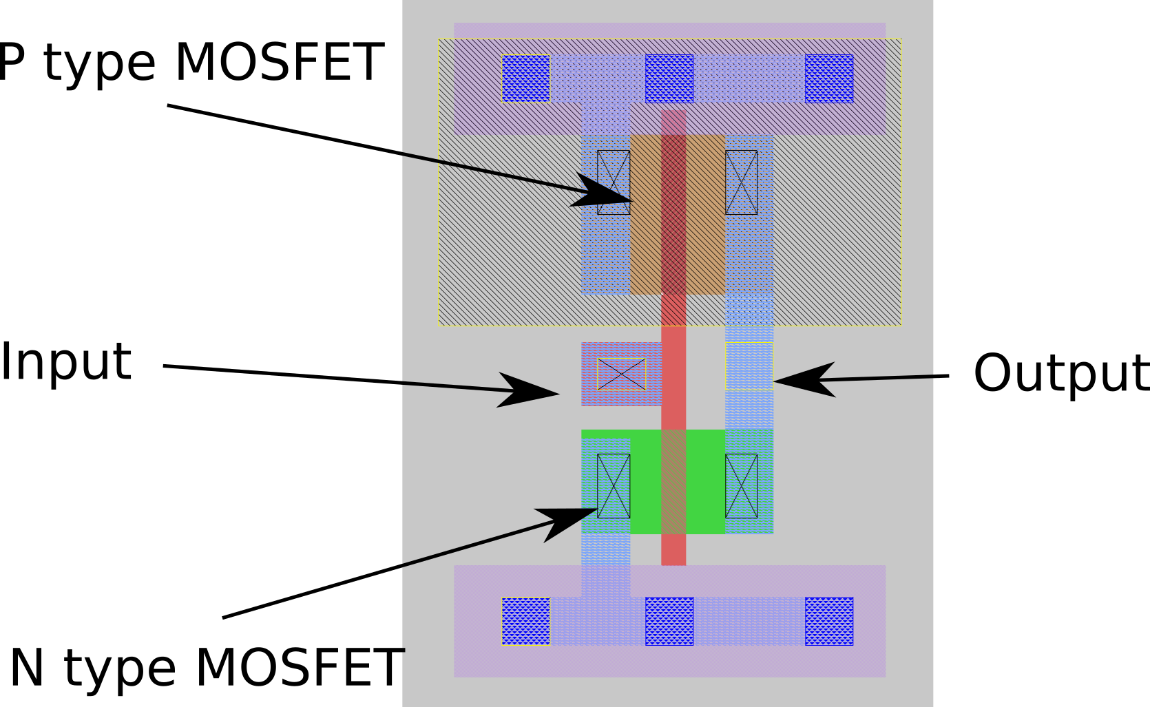
This video shows a sped up screen capture of me laying out a DRC clean inverter with Magic.
Course feedback
The course was very interesting, and the knowledge I obtained has proven to be very useful. It's great how accessible fabrication has become thanks to TinyTapeout and SkyWater 130.
Eduardo Holguin (digital course)