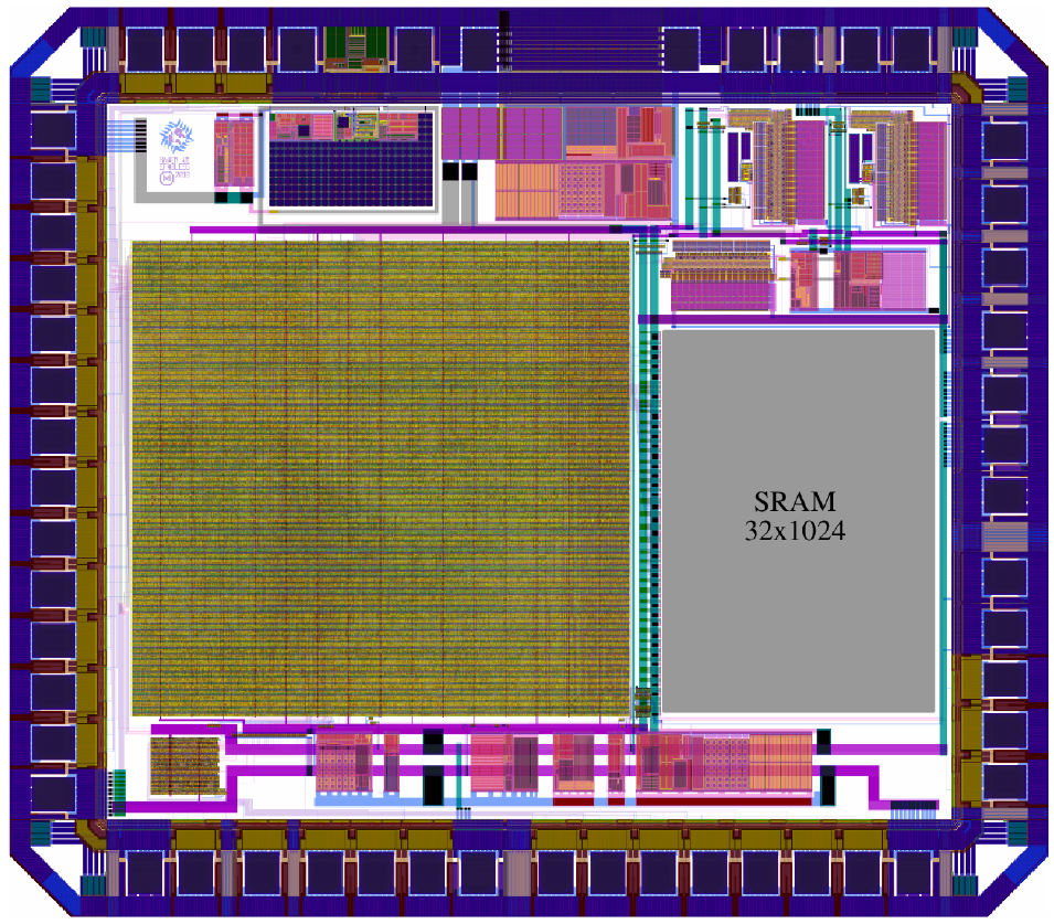
Padring
We need to make sure we can package the IC after the wafer has been diced into individual dies.
A common way of packaging ICs is to connect them to a leadframe by bonding tiny wires between the leads of the leadframe and the pads on the die.
The big bond pads around the outside of the IC often include ESD protection diodes, Input/Output drivers and so on.
This picture shows raven, an IC from Efabless. You can see around the edge there are the big bond pads and the power and ground lines. This structure is called a padring.
The padring used in the Google shuttle is included in Caravel.
Course feedback
This course is really valuable, especially university students like me. I really wished I could have got access earlier, I just didn't know about it.
Anderson (digital course)