Wafer
Silicon is purified to around 99.9999999%! Then it is sliced into very thin round sheets called wafers.
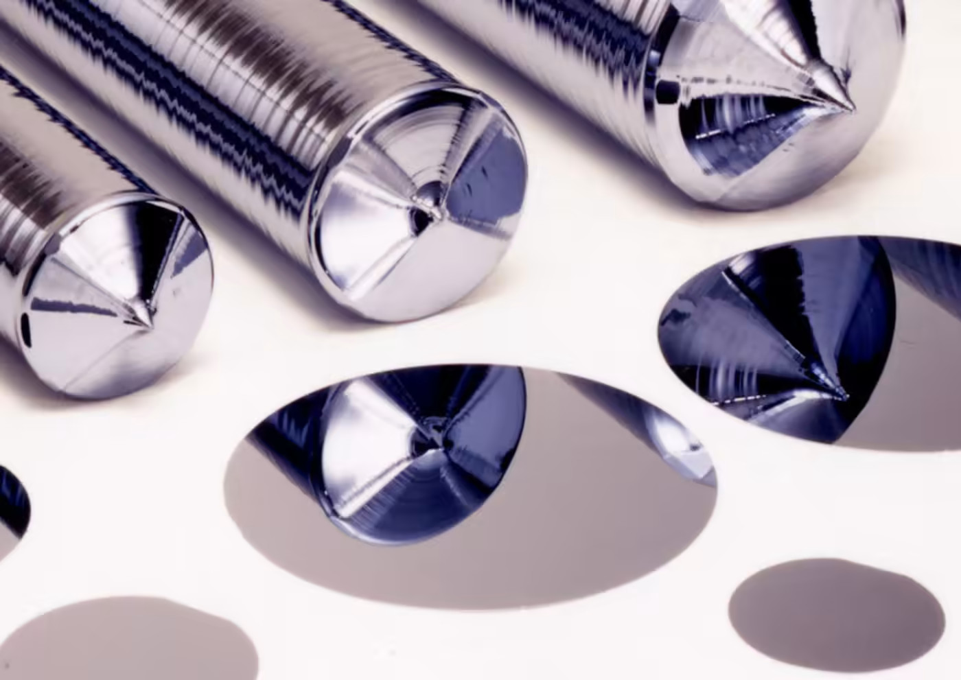
The type used in the Skywater 130nm process is doped to become p-type.
Here’s a great video about how silicon wafers are made.
And these great videos are about the birth of the Japanese semiconductor industry. Jump to about 12 minutes in to see how they pull the silicon ingot out of the molten material.
After the wafers are ready, they can be patterned using the photolithographic process, using a series of masks.
Course feedback
The really exciting part for me is when you see what you've written actually end up as laid out digital logic.
Robert Baruch (digital course)