Die
The silicon wafer is usually patterned with the mask set to make hundreds or thousands of the same IC. The circle below represents the wafer, the squares represent the copies of the maskset pattern exposed onto the wafer by the stepper. The light squares are completely within the wafer and thus may be functional chips, the others are only partial and so cannot be functional chips.

Each of these ICs are then cut out of the wafer using a diamond edged saw and are called dies (or die, or dice).

The die is then somehow packaged. Often they are mounted to a leadframe and then moulded into a plastic packaging to make them larger and easier to handle.
Typically, the separated die are tested at this stage, and the faulty ones marked. Only non-faulty ones would then be assembled into packages.
Leadframe
The chip or die would be attached to the central square area of the lead frame with an epoxy glue, then bondwires would attach the pads of the die to the corresponding lead of the frame. The whole leadframe then goes into an injection moulding machine to encapsulate the individual die, four sections of black plastic for this case, then the leadframe is chopped and the leads formed into legs for the finished product.
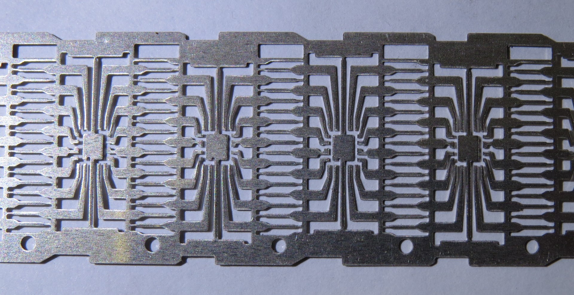
Image from Sergei Frolov
Read more about how the dual in line package was created (DIP) in this Hackaday article
The Google shuttle will provide a type of packaging called Wafer Level Chip Scale Packaging.
Course feedback
This course has fundamentally changed how I will teach VLSI in the future. Having used and taught the closed source tools, I am now a convert to the open-source tool chain. This course was the guiding force to get over the initial hump of the learning curve near painlessly.
Devin (analog course)