Place and Route
Place and Route are two steps in the automated process of turning some HDL into GDS2 files. We will look at how LibreLane does these steps using the seven segment seconds example.
I have used my presentation tools to generate these images.
Place
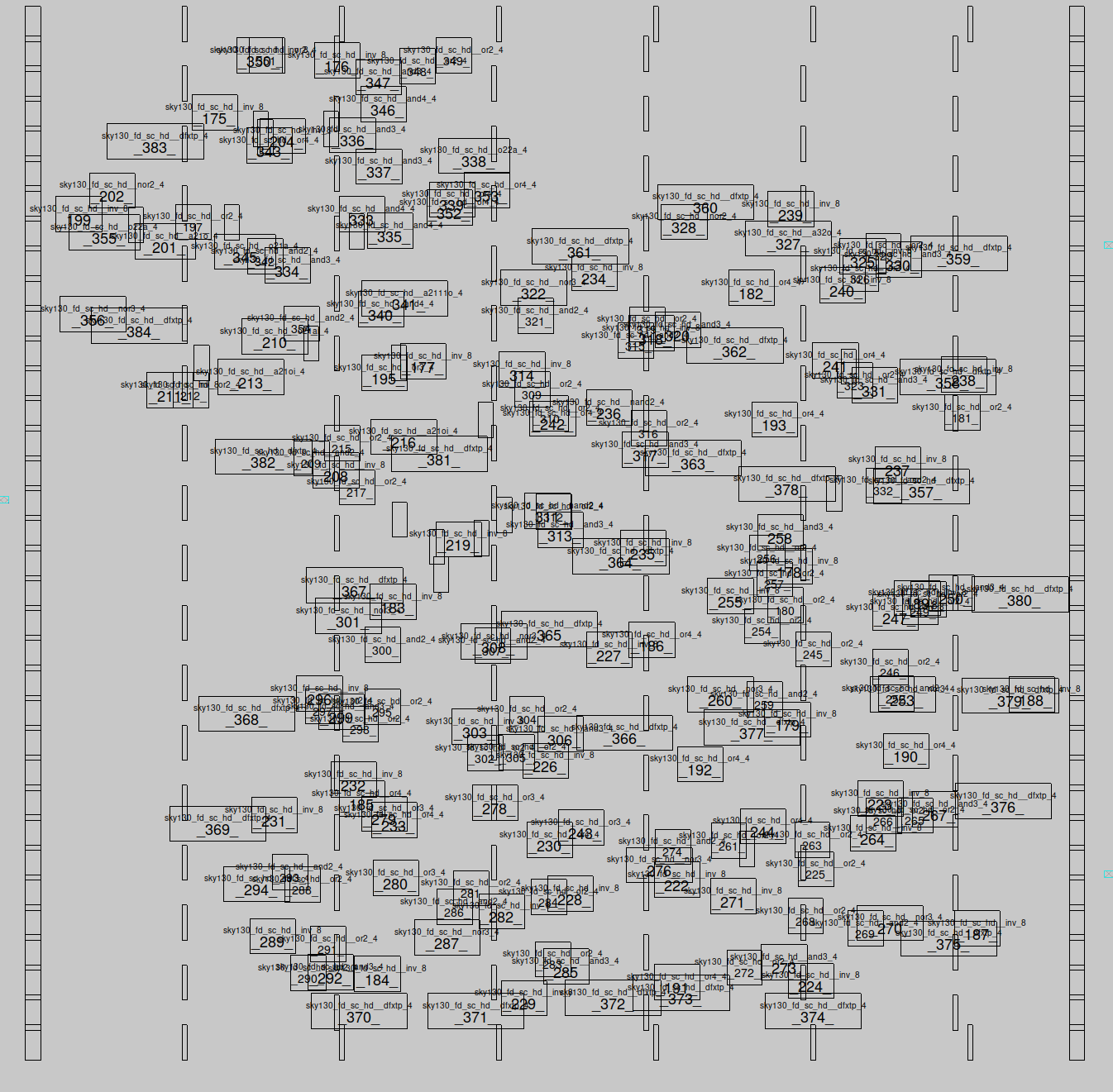
Placement is done in two steps, coarse and fine. The coarse step puts the standard cells in roughly the right place. This may be referred to as global placement, or initial placment. The aim here is to minimise the estimated total wire length of all the nets in the design, while ensuring that in any given area there are not more cells than will ultimately be able to legally fit. There are many techniques used in placement, but the simplest tries to find which instances are each side of a dividing line so that the number of wires crossing that line is minimised and the total area of cells on each side is roughly equal. By repeating this bisection process many times, we end up with a small number of cells in each small area, and can then rearrange them to further reduce the local and global wiring length.
The file shown is replace.def.

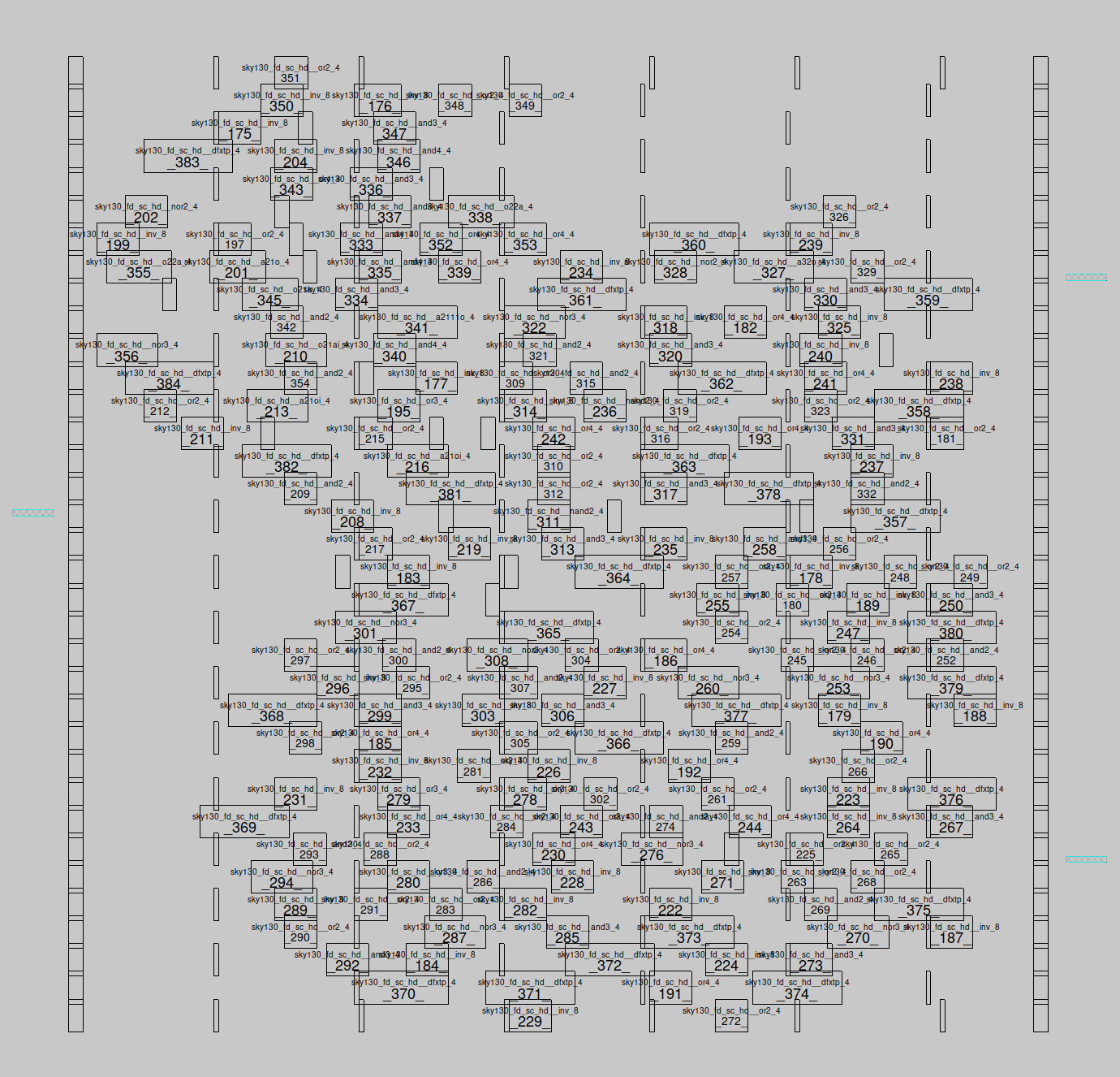
The fine step aligns the cells to the grid and makes sure they don’t overlap, while trying to reduce or limit the wiring length. This step is often referred to as ’legalisation'.
The file shown is placement.def.

Route
After the cells are in the correct places, the routing of clocks, power and signals can start.
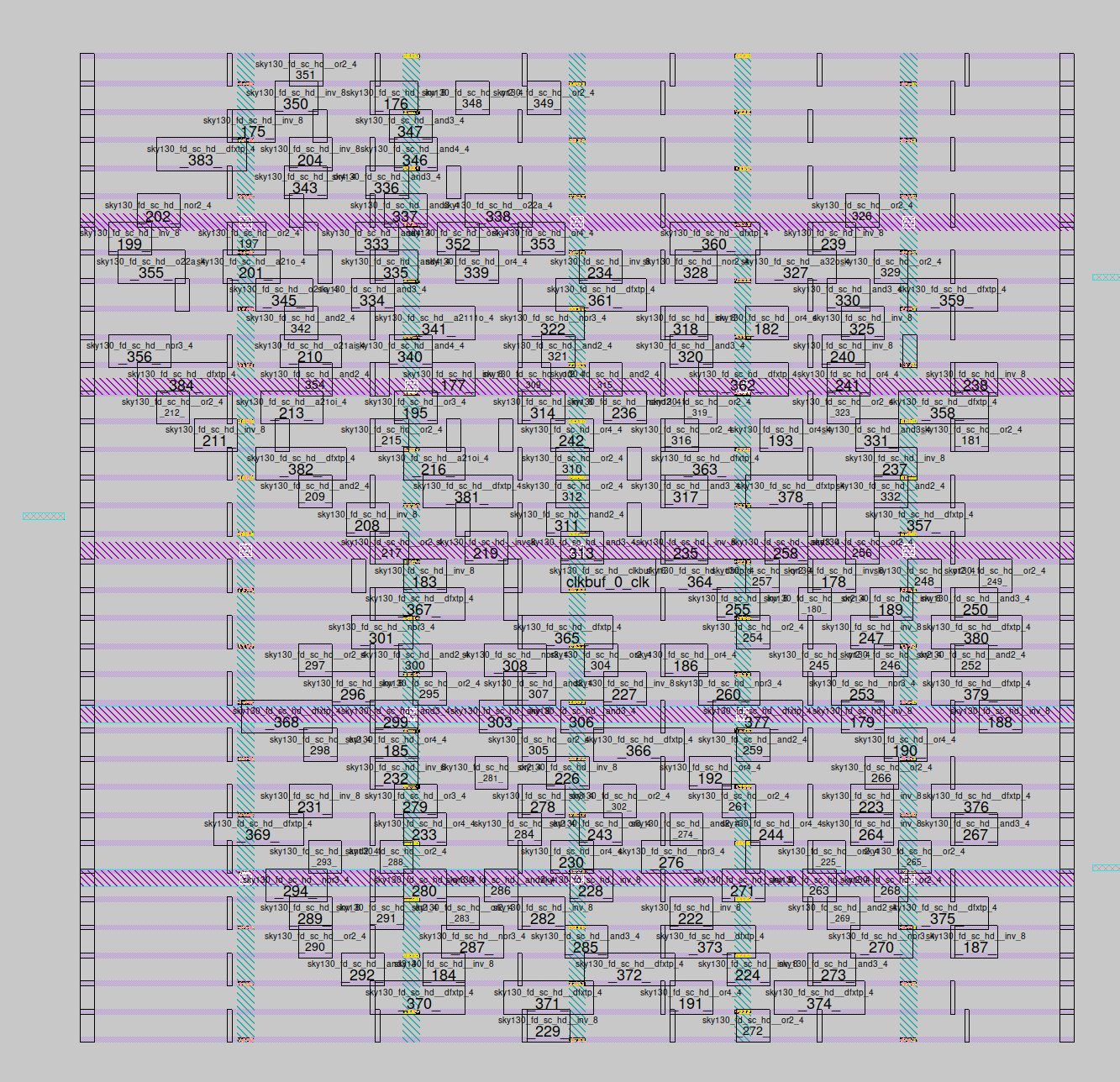
Here is the power distribution, the file shown is pdn.net. You can see thick horizontal metal lines carrying power and ground. Then there are the thinner horizontal lines that connect to the top and bottom of the standard cells. That’s why all the standard cells have the power and ground at the top and bottom at a fixed distance. Most of the power distribution is performed by the rails inside the standard cells of the user’s design, and the filler cells that are inserted in the gaps between them. The distibution network then feeds power to these rails and tries to ensure that all cells see the same voltages.
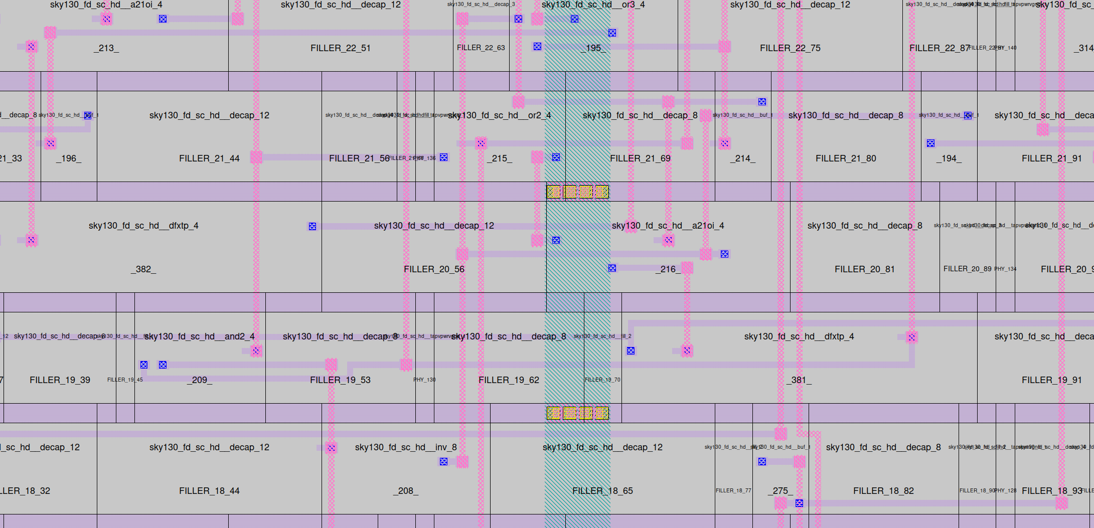
The rest of the signals can be routed using a variety of techniques, typically based around a localised maze routing algorithm, potentially guided by a global routing analysis step.

And finally, here is a zoomed image of the same design, but showing the routing wires on the metal layers. This file is routing/design.def

Clock Tree Synthesis
I don’t have a good picture of CTS, but it’s worth mentioning here. The clock (and reset) are important and heavily loaded signals. The clock especially is probably driving thousands of gates. Each of these gates has a small capacitance that requires some effort to charge or discharge. For this reason the clock line is treated specially and CTS makes sure the clock drive strength is strong enough by adding special clock buffer standard cells. It is also important that all flip-flops attached to the clock see similar signals, meaning that the delay from the clock source and the edge rates are very similar at every point. If this is not the case then the skew between the clocks arriving at two flip-flops will impact the available time to get a signal between those flip-flops. If the later flip-flop has the earlier clock, then that means the path between the flops has less time to execute, and this may mean that we have to slow the clock supplied to the whole chip down in order for it to work. If the clock to the second flip-flop is the later clock then there is a risk of a hold violation, meaning that it will process data in the wrong order and this can mean that the chip is non-functional at any clock speed. CTS aims to reduce the total clock source to flip-flop delay, and minimise the skew of all signals delivered to all the attached flip-flops, while controlling the amount of added circuitry (and wiring) used.
Course feedback
Having studied analog theory in college but not having the opportunity to tape out left a void in my heart. This course really was the “missing semester” for taping out analog and mixed signal designs. I highly recommend it anyone who wants to bridge this skill gap!
Argunda (analog course)