ASIC Necklace
For the last few years I’ve worn an old 4 inch wafer to conferences or whenever I’m teaching in person. People rarely get to handle a wafer and are always interested to know more.
While it’s a fantastic conversation starter, the problem with this necklace is that it’s too hip-hop, and not enough “15 million dollar Nikon Lithography Stepper”. To resolve this annoyance, I decided to make the most ridiculous ASIC bling possible - using my own chips of course! The only thing I kept from the old design was the quick release wafer.
A project like this needs a great team - and I got lucky with Pat Deegan and Adam Zeloof.
Read on to follow the development story, go straight to the photos or watch the video.
Concept Design
I started with some concept sketches in August 2023. I always prefer paper and pen for the first sketches, much faster for me than working with a computer.
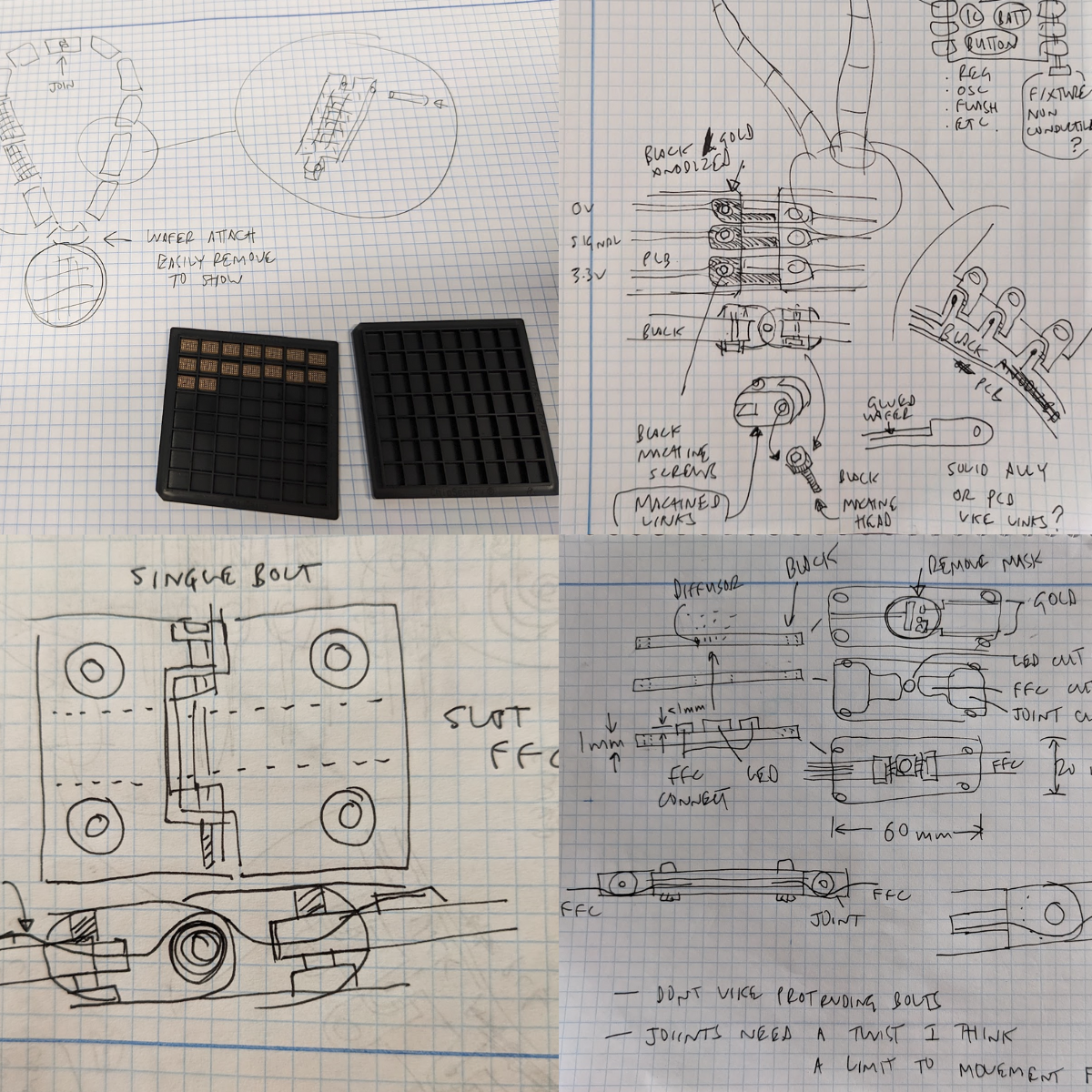
The challenging part was making strong, flexible, conductive and most importantly - good looking links.
After a few iterations we decided on gold anodized CNC aluminium links held between sandwiches of black PCBs. The top PCB acts as a decorative light diffusor while the bottom holds the LED and passes the signals around the chain.
3D design
Adam did the design with Onshape (account needed to view the design), a web based CAD tool. I was able to view the design, give feedback and make measurements all inside my browser.
We realised that the edges of the PCB sandwiches wouldn’t look great so Adam designed a spacer that holds the top and bottom PCBs apart while covering the sides of the boards. The bottom boards have a surface mount soldered nut and the top board is screwed on with some nice low profile machine head bolts.
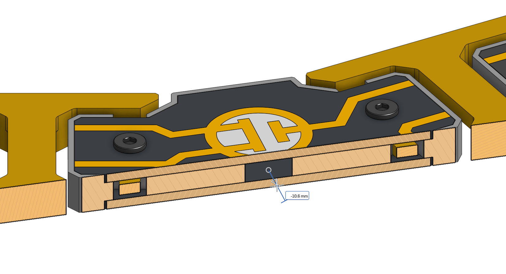
The spacers are black nylon printed with Multi Jet Fusion, a technique that results in an industrial look and feel. Adam used this technique a lot when he worked at Boston Dynamics.
Decorative pattern
I knew I wanted something that represented a MOSFET, as they’re fundamental to all my chip design so far. I also liked the idea of showing a simplified circuit diagram that represented the hidden electronics inside the chain.
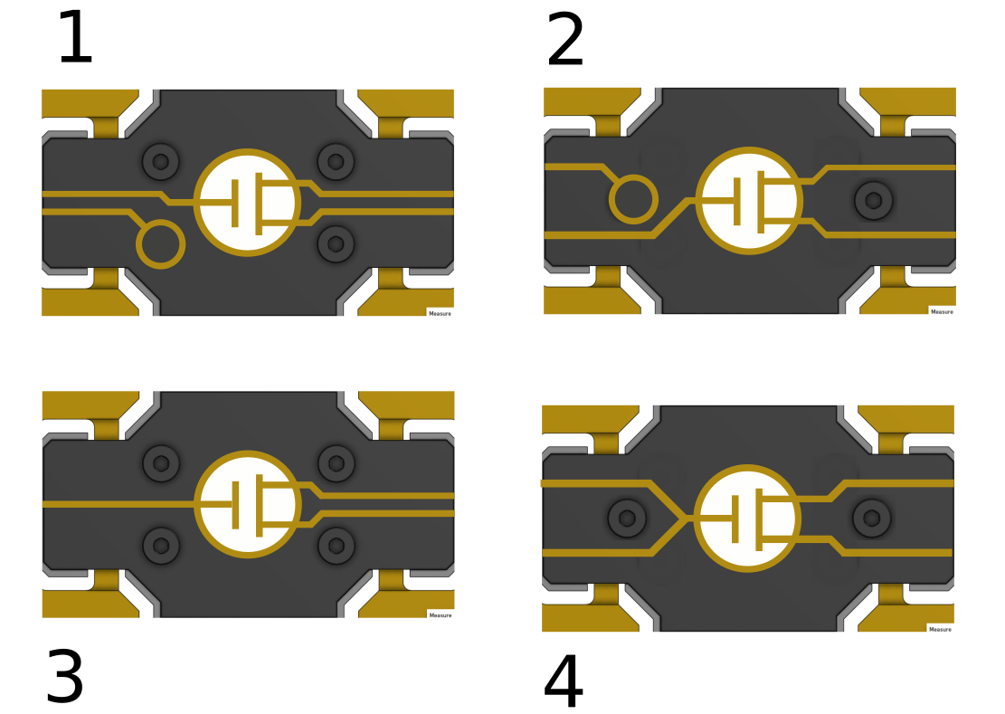
I was really struggling to come up with a design that I was happy with, but finally Adam came up with something that was proportional to the link, looked good and connected a 3 pin device to a 4 symmetric wires. Yes I know MOSFETs are 4 pin devices. No, I couldn’t get it to look good in the space we had - some artistic license was taken!
Diffusion
LED diffusion is crucial to a high-class blinky. Pat did some testing with the LEDs to see how they’d diffuse through the PCB. We measured the diameter of the light hitting some layers of paper held over the LED and used that for the diameter of the logo.
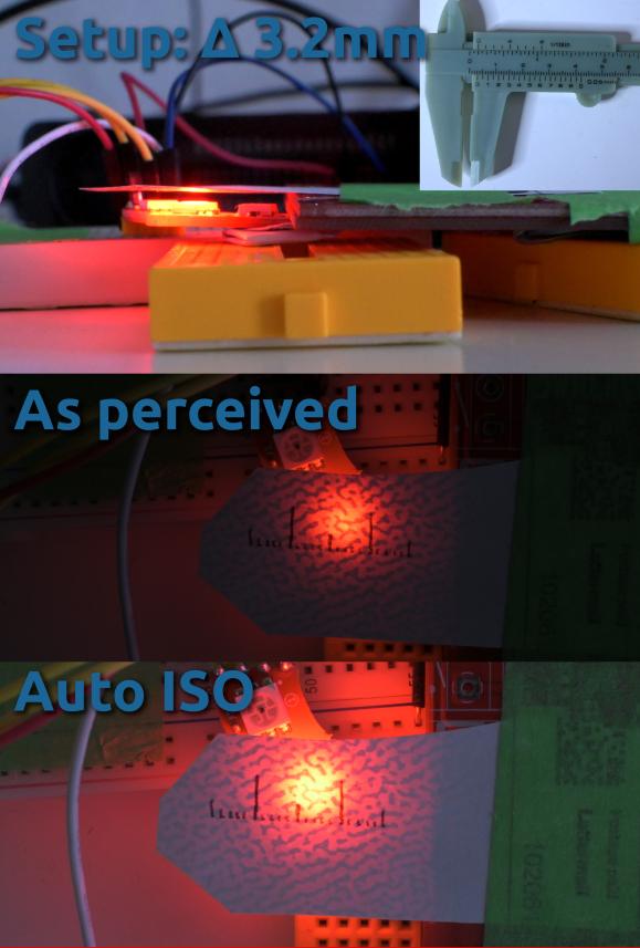
We blocked the light by covering everything outside the logo with copper, draped the copper with the mattest of matte black soldermask and topped it all off with stunning gold plated traces.
Electronics
The chips I used were extremely rare, an exclusive 2022 vintage we submitted to Efabless chipIgnite.
Unlike my first ASIC it doesn’t contain my WS2812 LED driver macro, so for the LEDs, I went with the easier to drive APA102s.
I used the chip’s on-board VexRiscv RISCV processor to bitbang the LEDs.
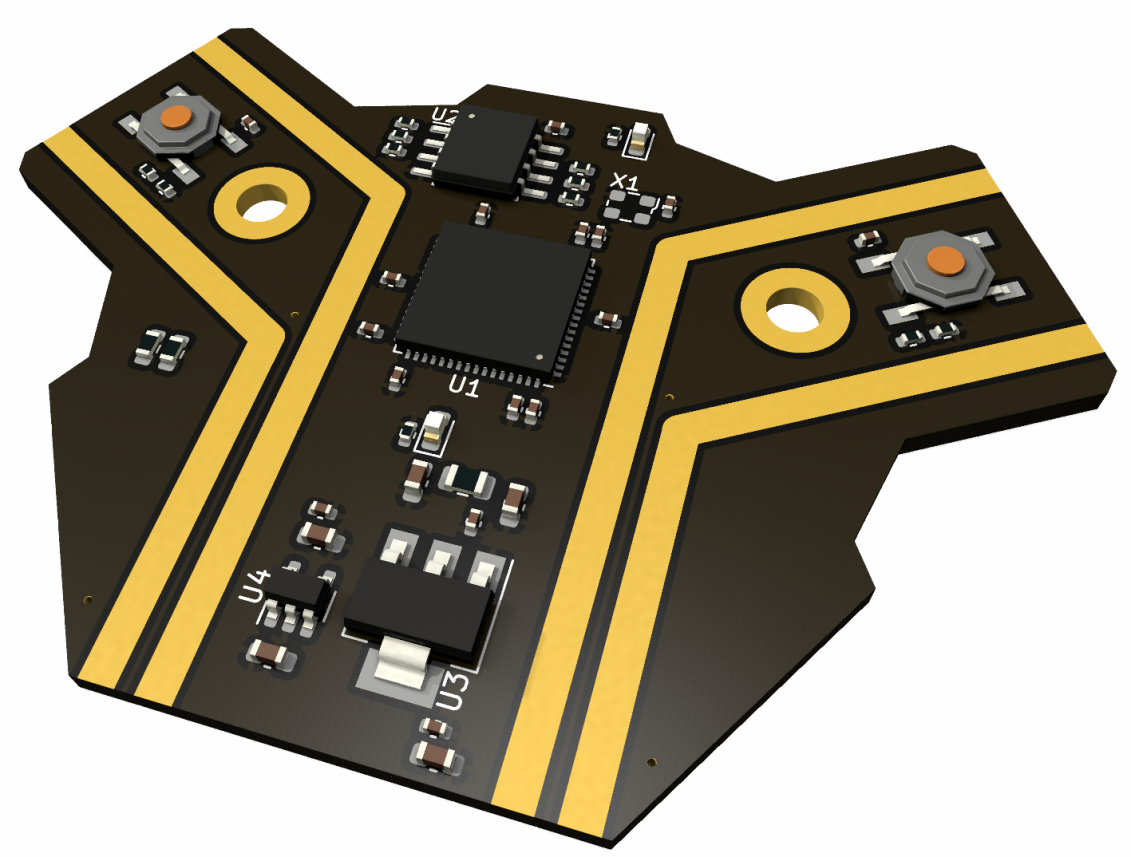
For the schematic we started with Pat’s minimal viable ASIC board. It’s a template schematic that includes all you need to boot a chipIgnite or Google funded MPW lottery chip. To customise it for the necklace we added a couple of buttons and some decorative stripes that serve double duty as capacitive touch sensors.
Pat did some very nice work on estimating power usage on the LEDs, and that helped us size the battery. The APA102’s datasheet says ‘Applied voltage 5VDC’, but we run them direct from the LiPo’s lower voltage and they work fine. We went with a 400mAh battery that lasts for a measly 2 hours. Always prepared, I keep some spares in my pocket and swap them over when no-one’s looking.
Ordering
I wanted to debut the necklace at Hackaday Supercon, and we very nearly didn’t make it. With just 24 days to go before the conference we started ordering parts 😬
- Aluminium links from Runzemetal on the 14th,
- Plastics from ? on the 22nd,
- PCBs from PCBWay on the 25th,
- Parts from Adafruit and DigiKey on the 25th.

Aluminium links and plastics arrived on the 31st and fitted well. Esden and Timon recommended Runzemetal after they did the beautiful case for Whitequark’s Glasgow.
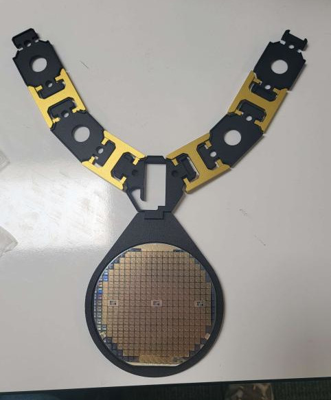
The PCBs went “out for delivery” on the 30th, but nobody actually showed up. Thankfully they arrived on the 31st and Pat pulled an all-nighter getting high on solder fumes to get it done before leaving for LA.
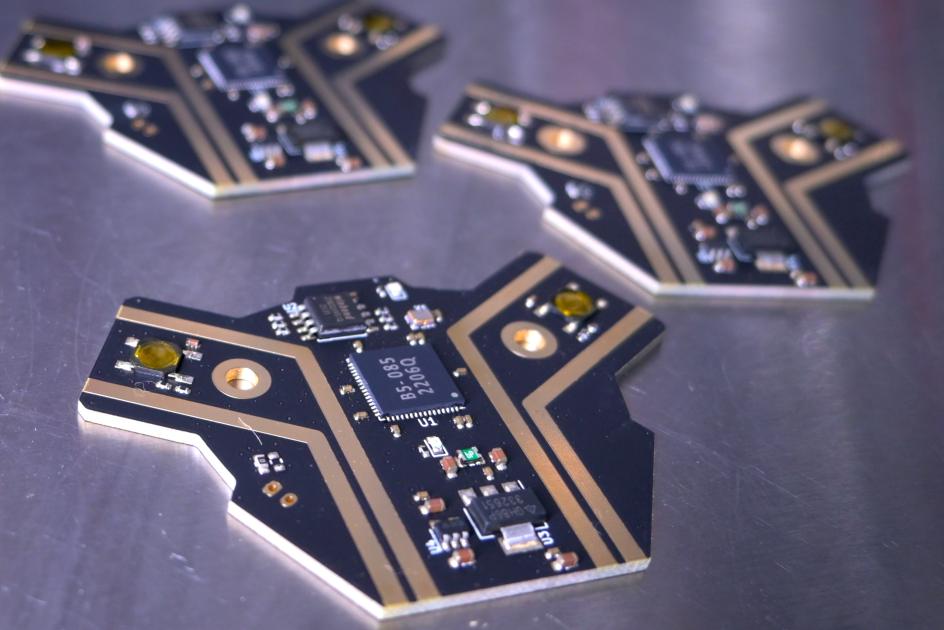
We got lucky everything arrived on time. We cut it so close it was tighter than two MOSFETs in a bitcell. Looking back, a bit more project planning would have been helpful. It wasn’t clear to us that we wouldn’t be able to order the PCBs until we basically had everything else finalised.
Assembly
Pat and I arrived in LA before Adam, and we tried plugging the links together for the first time and writing a quick firmware to control the lights. Amazingly it all worked, but the update rate of the LEDs was extremely slow. I decided to keep it simple with a solid green and a cold beer. As a future upgrade, I plan to animate the LEDs using one of the chip’s ring oscillators - to change the animation with temperature.
After my Tiny Tapeout workshop at the conference Adam arrived and we tried fitting it all together for the first time. Nail biting!
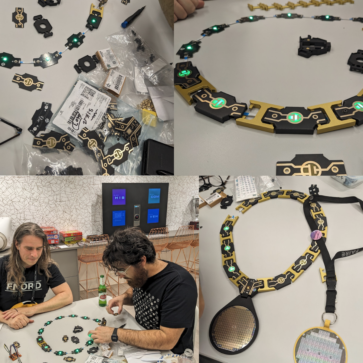
It came together really well, very good for a first assembly and also the first time we’d all worked together as a team. I’d like to pretend I knew it was all going to work first time, but in my experience it’s rarely the case.
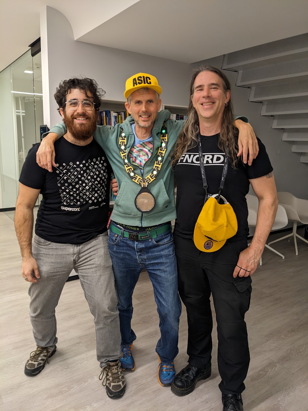
Wearing it at the con
At a princely 500 grams, it’s a lot heavier than my previous necklace. It took some time to get used to wearing it but now my necks bulked out I’m ok.
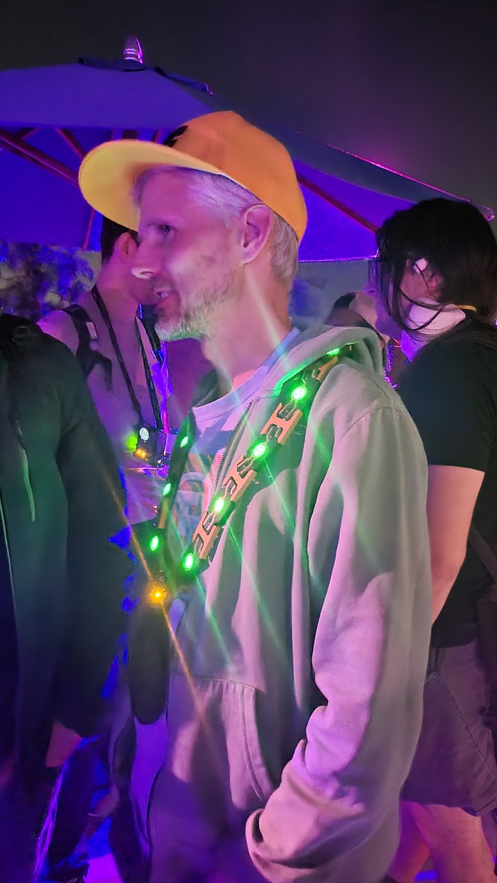
You might think I stood out, but the con’s blinky game was so strong I blended right in.
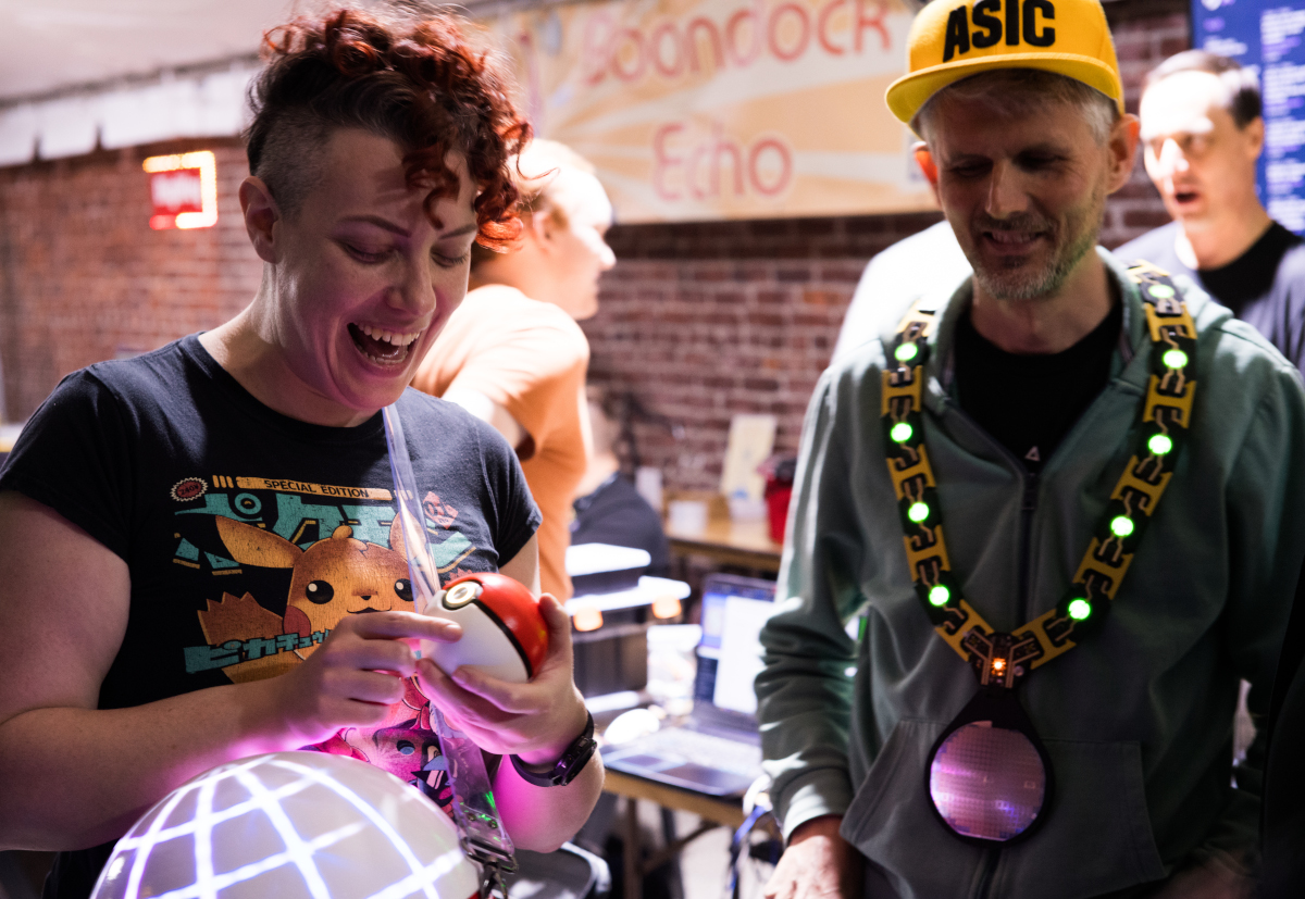
Improvements
Over the next 3 days we exposed some design flaws:
- The wafer clip was meant to be a snap fit, but it wasn’t quite snappy enough and the wafer fell off a couple of times.
- The clearance between the aluminium and the PCBs was meant to limit the chain to around 15 degrees of movement but it can actually move around 45 degrees.
- The FFC cables are too exposed and can get pulled out of their tiny sockets by the excessive chain flexing that often happens when I’m fighting other electronic super heroes.
We were never convinced by the FFCs so as consummate professionals we had designed in a backup: extra pads on the back of the boards we could just solder wires to. I executed a high pressure fix right before my interview with Make!
Photoshoot
Thanks to Bruce and Majenta at Supplyframe for letting me use the design lab’s CNC machines as the sexy backdrop.
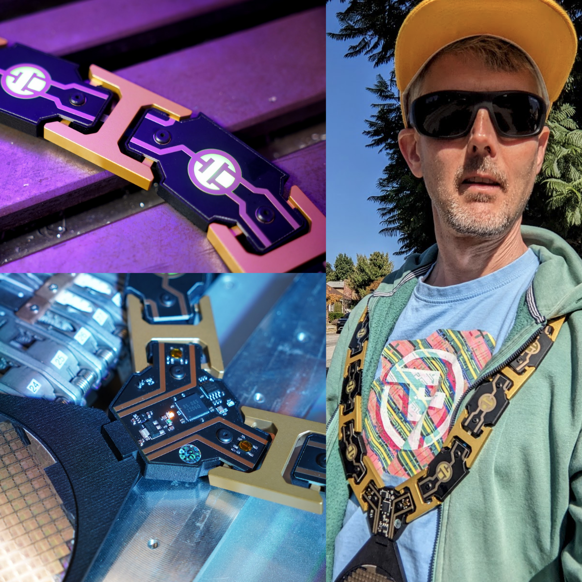
Now go and enjoy the high resolution gallery of my favourite photos!
Resources
The necklace is open source hardware and software, inspectable down to the transistors in the microchip.
- All the photos
- The necklace on Adam’s open jewelry site
- 3D CAD license CC-BY-SA-4.0
- Firmware license Apache 2
- PCBs repository license CC-BY-NC-SA-4.0
- OSHWA certification ES000042