Short articles about my experience with making ASICs, interviews and any other related topics I think are interesting.
ASIC Necklace
For the last few years I’ve worn an old 4 inch wafer to conferences or whenever I’m teaching in person. People rarely get to handle a wafer and are always interested to know more.
While it’s a fantastic conversation starter, the problem with this necklace is that it’s too hip-hop, and not enough “15 million dollar Nikon Lithography Stepper”. To resolve this annoyance, I decided to make the most ridiculous ASIC bling possible - using my own chips of course! The only thing I kept from the old design was the quick release wafer.
Tiny Tapeout 2 Silicon Is Alive!
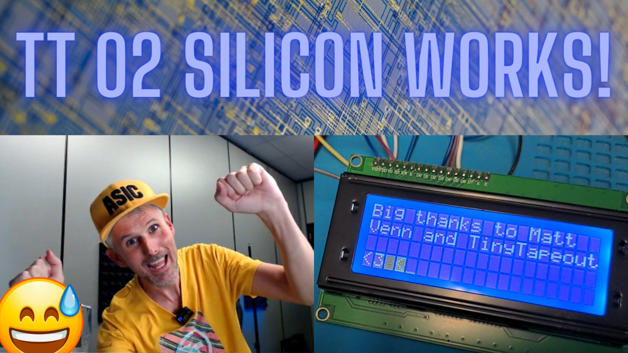
We submitted Tiny Tapeout 2 back in December, and last week I received the chips from Efabless.
Most first chip designs fail, but you never hear about it because the big companies keep it a secret. So we thought - why not do the world’s first public silicon bring up?
Thankfully the chips worked, and you can watch the whole stream here.
We’ve since found 1 errata, but luckily not a show stopper.
Tiny Tapeout 4
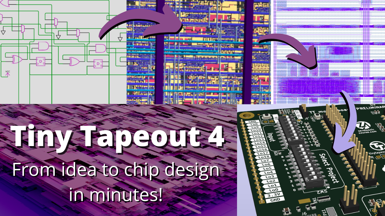
I’m very happy to have over 140 designs from 30 countries submitted to Tiny Tapeout 4!
Top level statistics:
- Total standard cells 82126
- Maximum cells used was 6813 for project 033
- Maximum utilisation was 87.18% for project 016
- Total wire length was 2607 mm
Thanks to everyone who submitted and all the contributors. Also a huge thanks to Efabless Corporation for sponsoring the project!
Tiny Tapeout 5 is already open and will close in early November 2023.
Free Silicon Conference 2023
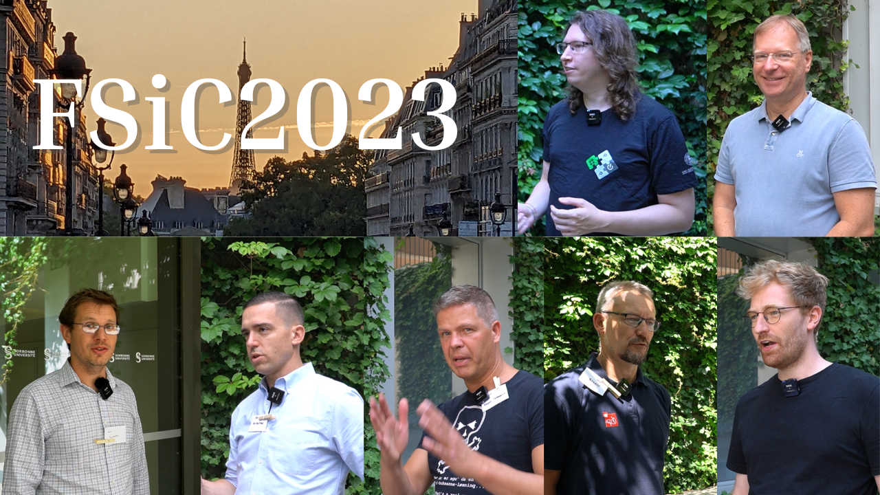
The Free Silicon Conference returned to Paris in 2023. There were plenty of great talks and I really enjoyed the conference. I was able to interview the organiser and several speakers:
- Luca Alloatti - organiser
- Thomas Benz - PULP
- Jørgen Kragh Jakobsen - his work on open source silicon in Denmark
- Thomas Parry - startup founder of Spherical Systems
- Rene Scholz - Open source PDK from IHP Microsystems
- Dan Fritchman - Analog tools
- Harald Pretl - Mixed signal design
You can find all the recorded talks here.
Looking inside my first ASIC with a particle accelerator
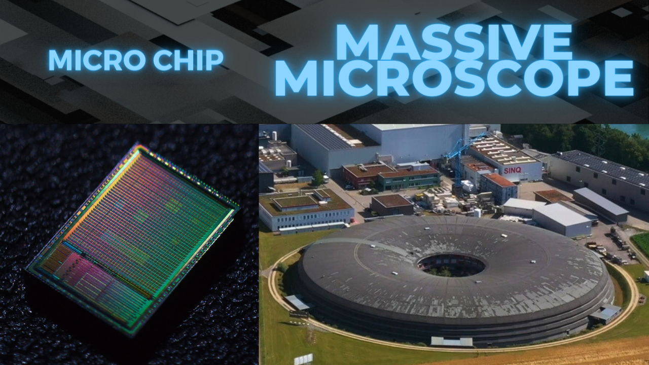
I got a once in a lifetime chance to use a particle accelerator to look inside my first ASIC!
It was amazing to be able to see all the different layers and match them up with the design files I sent to Efabless.
So join me on my journey to the Swiss Light Source at the Paul Scherrer Institut where I learnt how they use their synchrotron to make some awesome images!
I also have a public photo album if you want some SLS themed wallpaper!
The MOnSter 6502 - a 6502 processor out of discrete transistors
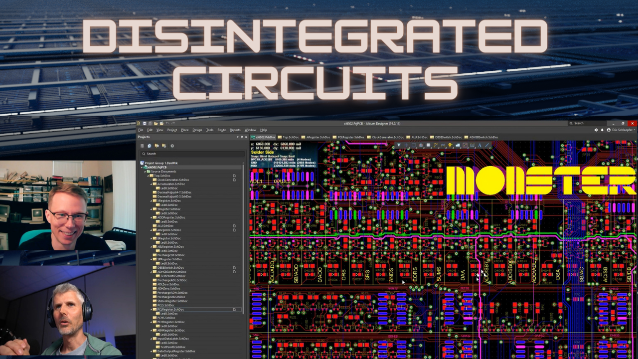
I had the chance to interview Eric Schlaepfer about his MOnSter 6502, a 6502 processor made out of discrete transistors. For me, one of the most interesting things about this project are the similarities to ASIC design, for example Eric wrote his own LVS tool.
You can find out lots more at his website.
Analog with Digital Standard Cells
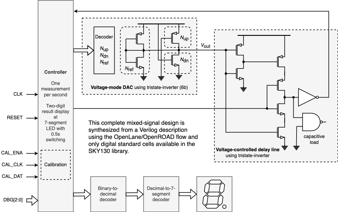
Harald Pretl made a fascinating submission to Tiny Tapeout 3, an analog circuit made from digital standard cells.

It builds a DAC out of a lot of tristate inverters, and a big capacitor by ganging up a lot of NAND gates.
In this interview with Harald we discuss how it works and how he made it and simulated it.
You can check his design here, including the source and GDS.
OpenROAD GUI
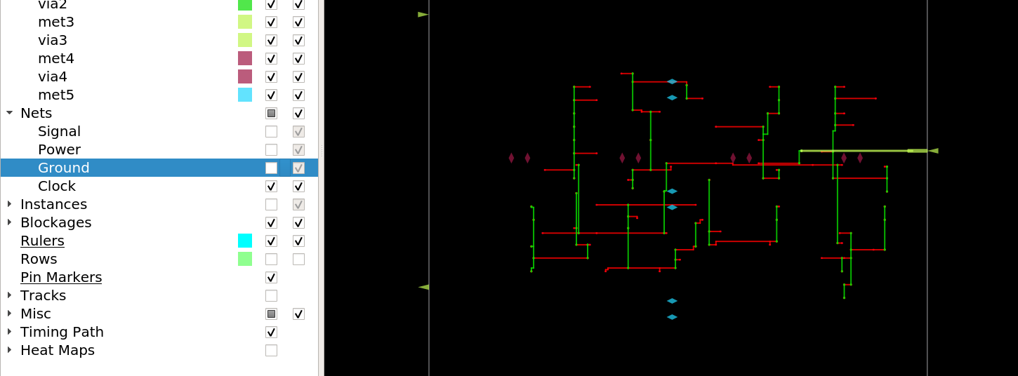
The OpenROAD GUI is a great way to explore your ASIC design. You can:
- View various types of heatmaps, including
- Placement density
- Power density
- Routing congestion
- IR drop
- Trace nets,
- View the clock tree,
- Inspect timing and more.
I recently spoke with Matt Liberty, and OpenROAD maintainer, and he showed me how to inspect a simple design.
OpenLane
If you’re using OpenLane to harden your ASIC designs, and you want to use the GUI, you might hit a segfault. If so, you’ll need to modify the OpenLane top level Makefile.
Review of 2022 and aims for 2023

Welcome to my highlights from 2022! It was a big year for open-source silicon, especially the Zero to ASIC course and Tiny Tapeout. Let’s look at some of the highlights and then some aims for 2023.
Here are a few of the highlights:
- Four Zero to ASIC course tapeouts: MPW5, MPW6, MPW7, and MPW8
- Rolled out Tiny Tapeout 1 and 2, helping nearly 250 people tapeout their designs,
- I personally submitted my 19th tapeout
- Presented and hosted a Tiny Tapeout workshop at the Hackaday SuperCon in Novemeber 2022. Met tons of people, including Sam Zeloof @szeloof.
- YouTube Channel had 82k views and 2.5k new subscribers
- Introduced Siliwiz
Zero to ASIC course Tapeouts
The Zero to ASIC course continued to grow, we now have 280 students and made submissions to four multi-project wafers (MPW).
Cloud Tools for ASIC Development
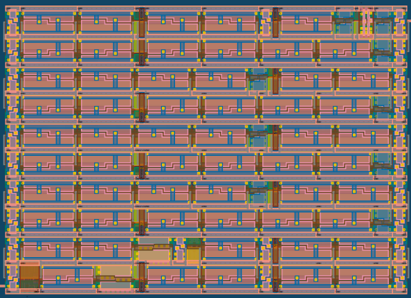
ASIC development tools have often been inaccessible due to cost and complexity. Even as free, open-source tools have become available, the complexity of building and installing the tools has slowed their use by would-be designers.
A challenge in making ASIC development more accessible has been to provide free, easy-to-use development tools. Thankfully development of cloud-based tools using open-source software are making chip design easier than ever.
In June 2022, I had the chance to talk with @Proppy, a Tokyo-based Google engineer who’s enabling people to collaborative ASIC in the cloud with Jupyter and Colab notebooks.