Short articles about my experience with making ASICs, interviews and any other related topics I think are interesting.
GlobalFoundries 180nm Fab
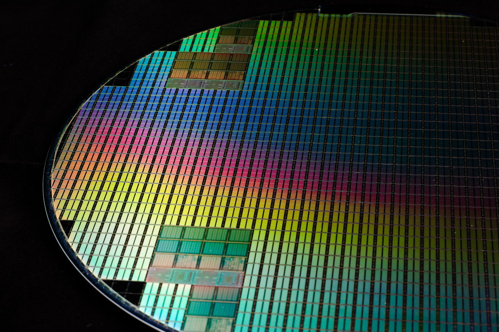
An exciting new opportunity for developing open-source silicon reached fruition at the end of 2022!
GlobalFoundries (GF) teamed up with Google to fund open-source projects using GF’s foundry and their open-source 180nm PDK GF180.
Open-source PDKs like GF180 and Skywater 130nm are essential for making silicon design more accessible. To now have GlobalFoundries involved with fabricating designs will hopefully mean increased opportunities to turn designs into silicon.
GF180’s first multi-project wafer (MPW) tapeout was in December 2022, and several people from the Zero to ASIC and Tiny Tapeout communities were able to submit designs. Here are some highlights:
Submit Tiny Tapeout Projects to an MPW
Using the Tiny User Project tool, people can quickly submit a Tiny Tapeout design to the MPW lottery. The low barrier to entry makes this a great tool to try variations on a design, test faster I/O speeds on an MPW tapeout, or simply compare tapeout processes using a different submission venue.
@Proppy developed the an easy-to-use tool as an extension to the Tiny Tapeout flow.
Proppy’s template repository uses GitHub actions to add a design to the Efabless Caravel User Project. The actions automatically perform the steps requried to harden the design, generate the necessary GDS files, and even generate a convenient GDS viewer. Additionally, the actions output useful reports on cell resource utilization, manufacturability errors, and the precheck results.
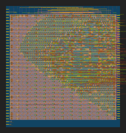
Tiny Tapeout 2 submitted for manufacture
I’m happy to announce that Tiny Tapeout 2 was successfully submitted for manufacture in December 2022! 164 designs were included on the tapeout.
Update! Tiny Tapeout 2 chips are back and working!
If you’re unfamiliar, Tiny Tapeout is an educational project that makes it easier and cheaper than ever to get your digital designs manufactured on a real chip! We had a first trial, Tiny Tapeout in September 2022 that was destined for MPW7.
Zero to ASIC course grant
I am excited to introduce a grant for the Zero to ASIC digital course.
The grant will provide a Silicon-level ticket for selected participants. Two grants will be awarded per month.
The grant is for people who are unable to pay the full price, please only apply if you need it.
Course goals
This course aims to revolutionize open-source silicon by training engineers, hobbyists and enthusiasts to make their own ASICs. During the course, you will design a circuit that will be submitted to Tiny Tapeout to be manufactured in silicon!
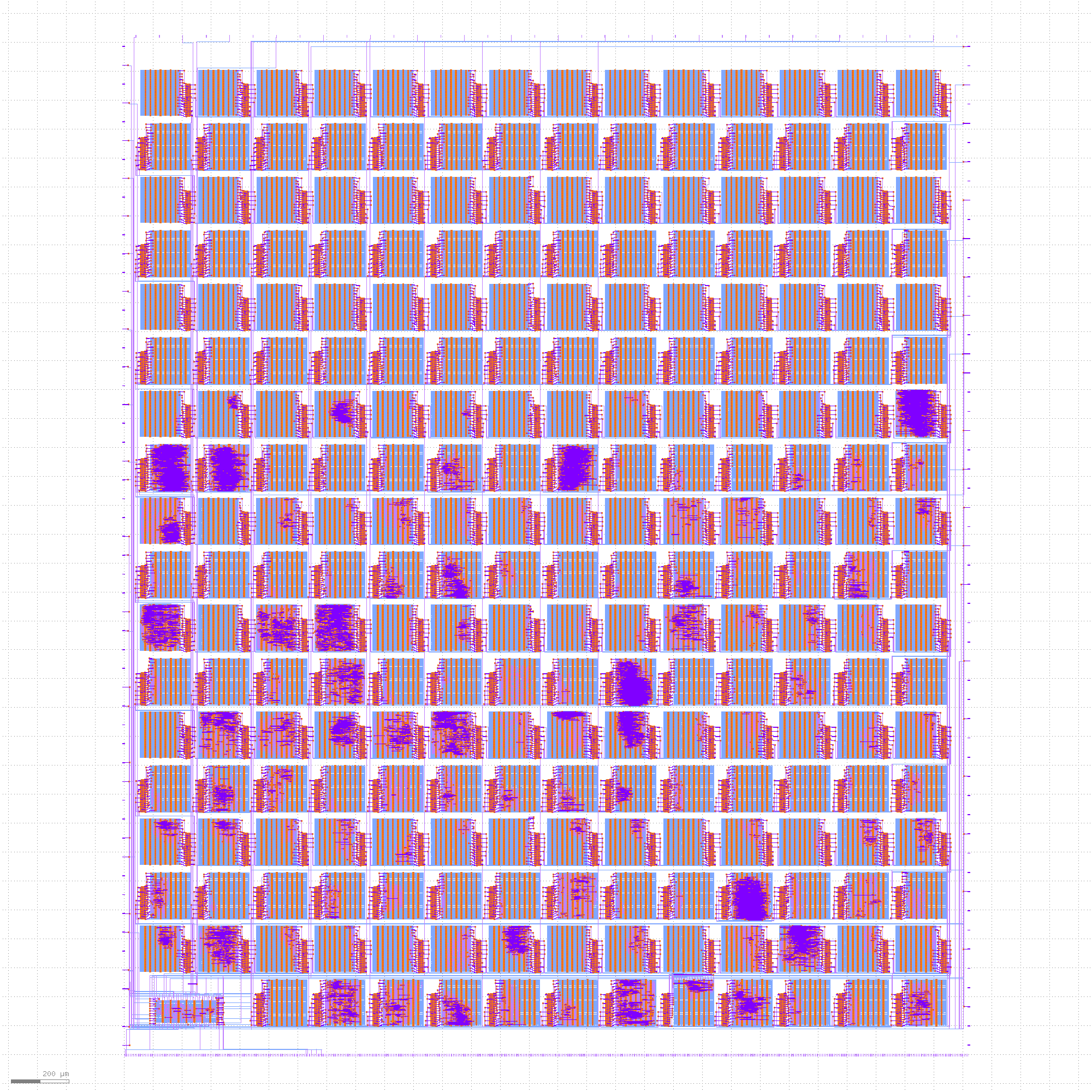
MPW8 submitted!
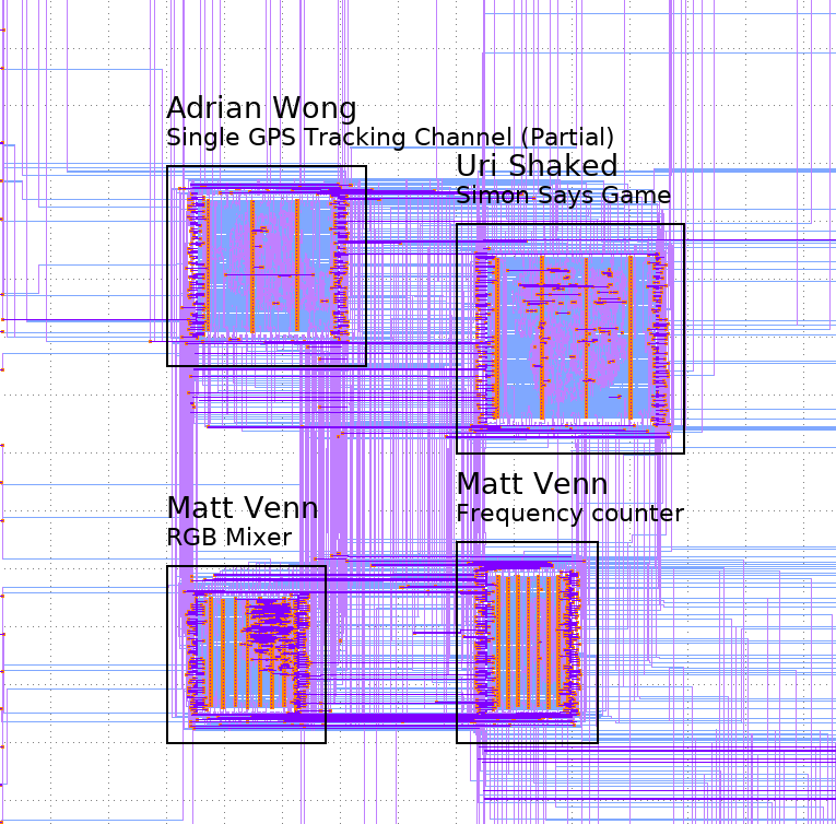
We submitted for MPW8! Special congratulations to Adrian Wong for the course submission!
We still managed to get 4 projects in the submission…not bad for a deadline of New Year’s Eve.
The projects include a partial implementation of an L1 GPS tracking channel by Adrian Wong, a Simon Says game implementated by Uri Shaked, and 2 demo submissions (frequency counter and RGB mixer) from me.
Here’s the github repo for the group submission and the Efabless project.
Become a Silicon Wizard with Siliwiz
SiliWiz will help you get a basic understanding of how semiconductors work and are manufactured at a fundamental level. It’s a free and open source tool that you can play with in your browser.
Aims
- Draw your own logic gate and understand how that gate would be manufactured in a foundry.
- Learn how the gate is built out of the fundamental circuit elements used in chip design
- Understand how the drawings are used to manufacture the chip
- Be aware of some of SiliWiz’s limitations and simplifications
Lessons
We have a set of free lessons that guide you through from drawing and simulating resistors all the way up to a CMOS inverter.
Monthly Update - September 2022
Welcome to the September 2022 monthly update!
Here are the main topics from last month:
- MPW7 submission,
- MPW2 updates,
- Job posting at E-Fabless,
- New videos,
- Is it the end for UVM? and
- Rendering GDS files with Blender or in your browser
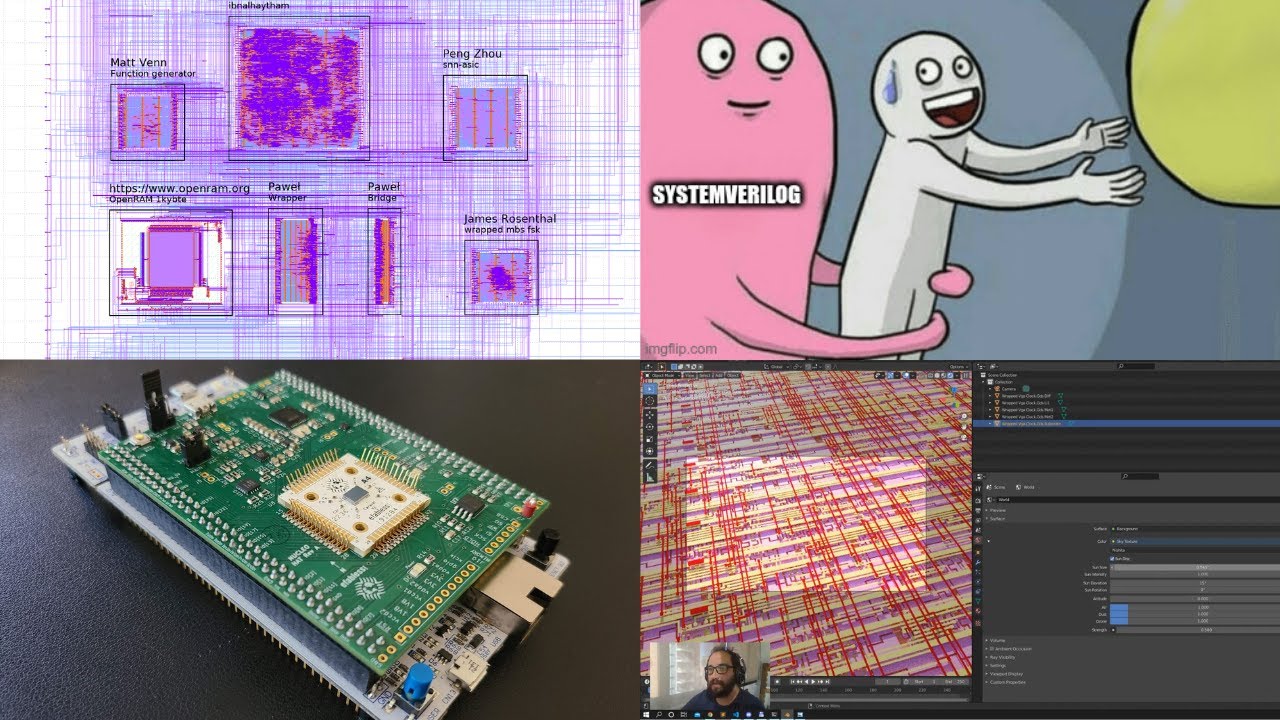
MPW7
The deadline for MPW7 was the 14th of September and the Zero to ASIC course submitted another set of projects. Special shout out to Farhad, Peng and James who are all first time tape outs on the project. Well done everyone!
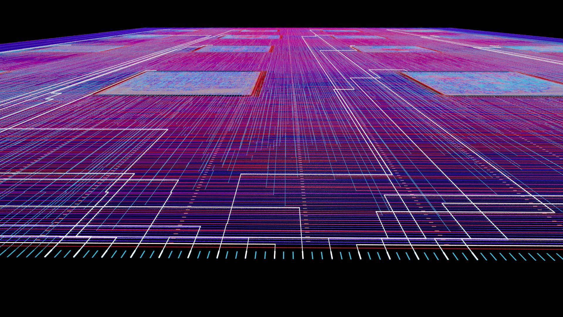
3D Rendering of GDS Files
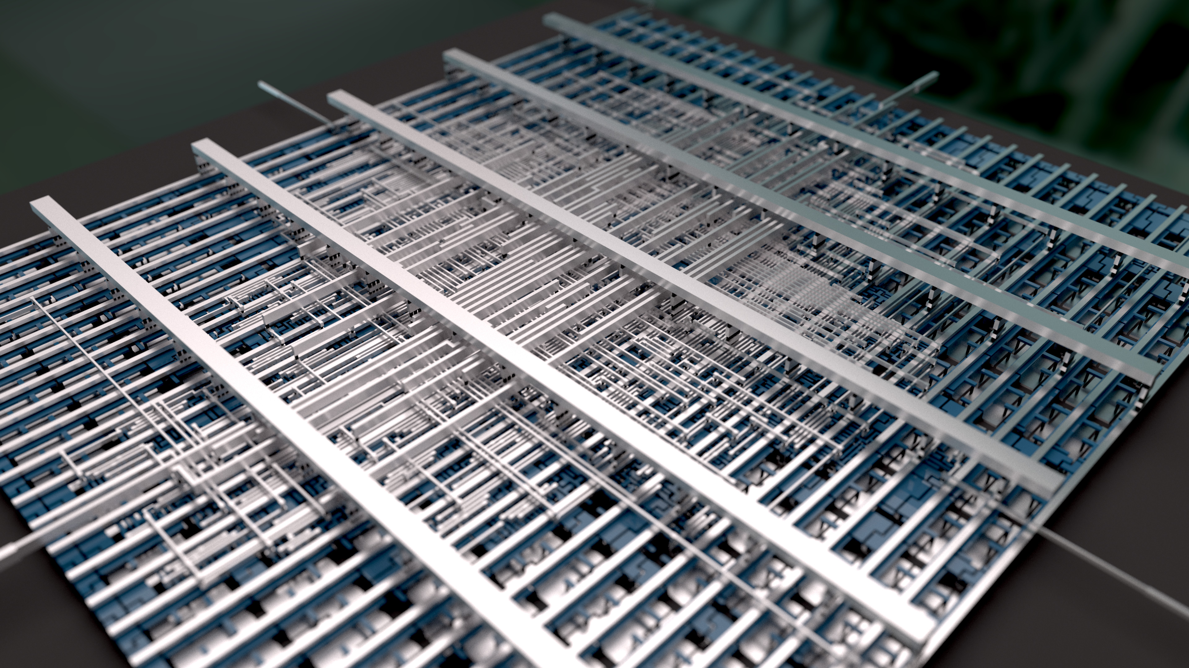
The 3D structures created within a silicon die are spectacular to see.
Thanks to Maximo (@maxiborga on Twitter), there’s now a video for 3D rendering ASIC designs enabling anyone to convert their ASIC design into a beautiful 3D rendering.
3D-rendered chip in Blender
His walkthrough shows how to convert GDS to STL files, enabling you to import the files in image editing software like Blender.
3D Printed Standard Cells
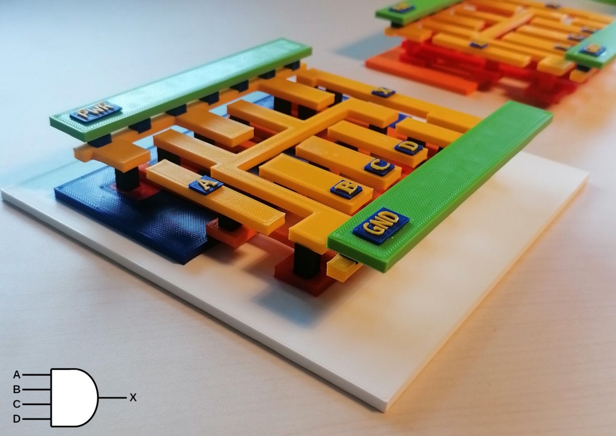
ASICs pack in billions of transistors per square centimeter, making their construction and functionality impossible to understand with the naked eye.
In fact, the upcoming 2 nanometer technology will be so small* that the transistor dimensions will only be 20X larger than an individual atom.
Wouldn’t it be great to see how ASICs are built in 3D at a scale that our bulky human hands can appreciate?
Well wait no longer! Thanks to Thorsten Knoll’s guide, you can now 3D print the cells that make up an ASIC using the GDS files.
Interview with James Stine - Open Source Standard Cells
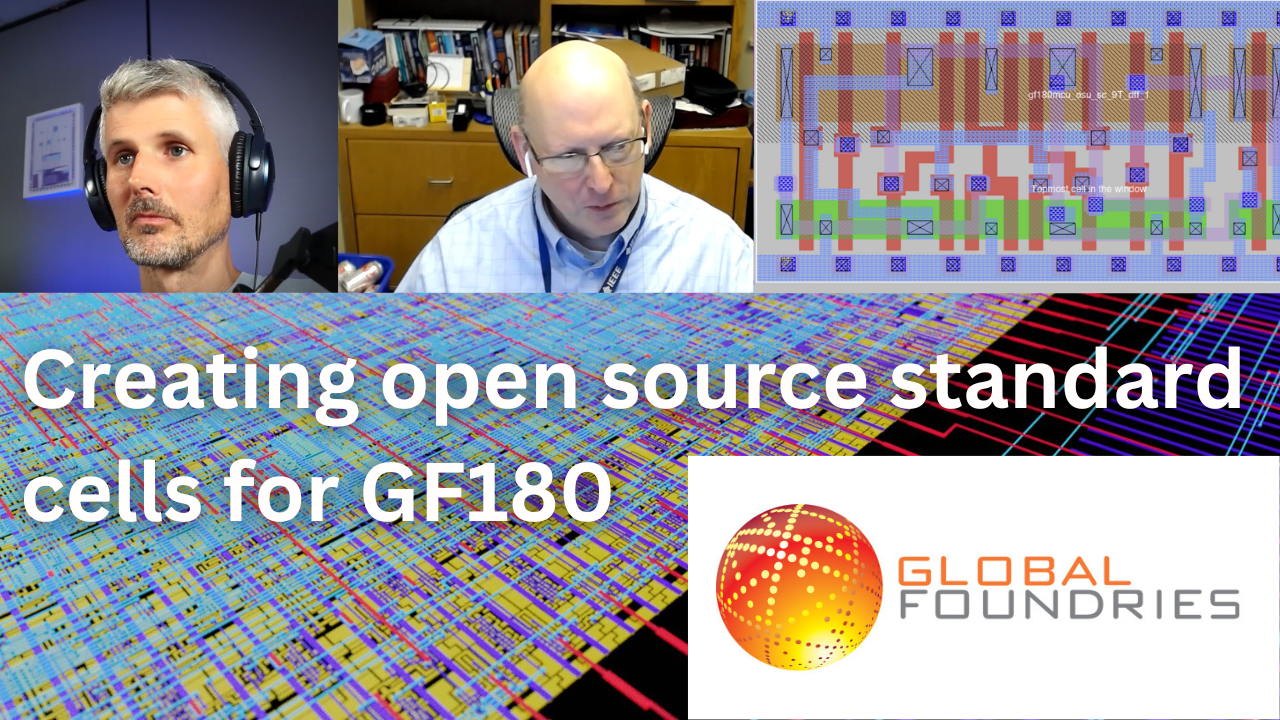
In this interview with Professor James Stine, we talk about:
- Why is Open Source the key to innovation?
- What do students struggle with most when learning to design standard cell libraries?
- What are the biggest misconceptions engineers have about standard cells?
- What’s James’ tool flow?
- How many cells are needed to make a library?
- Why do we need another library for Global Foundries (GF) 180?
- How far are open source tools from commercial tools?
- Could automated layout of standard cells compete with hand layouts in nanometer processes?
- With Moore’s Law slowing down, do any circuit families deserve a second chance?
- Why would nVidia make a 7.5T standard cell library?
Text of the interview is included below.