Short articles about my experience with making ASICs, interviews and any other related topics I think are interesting.
Interview with Lakshmi S - PLL design
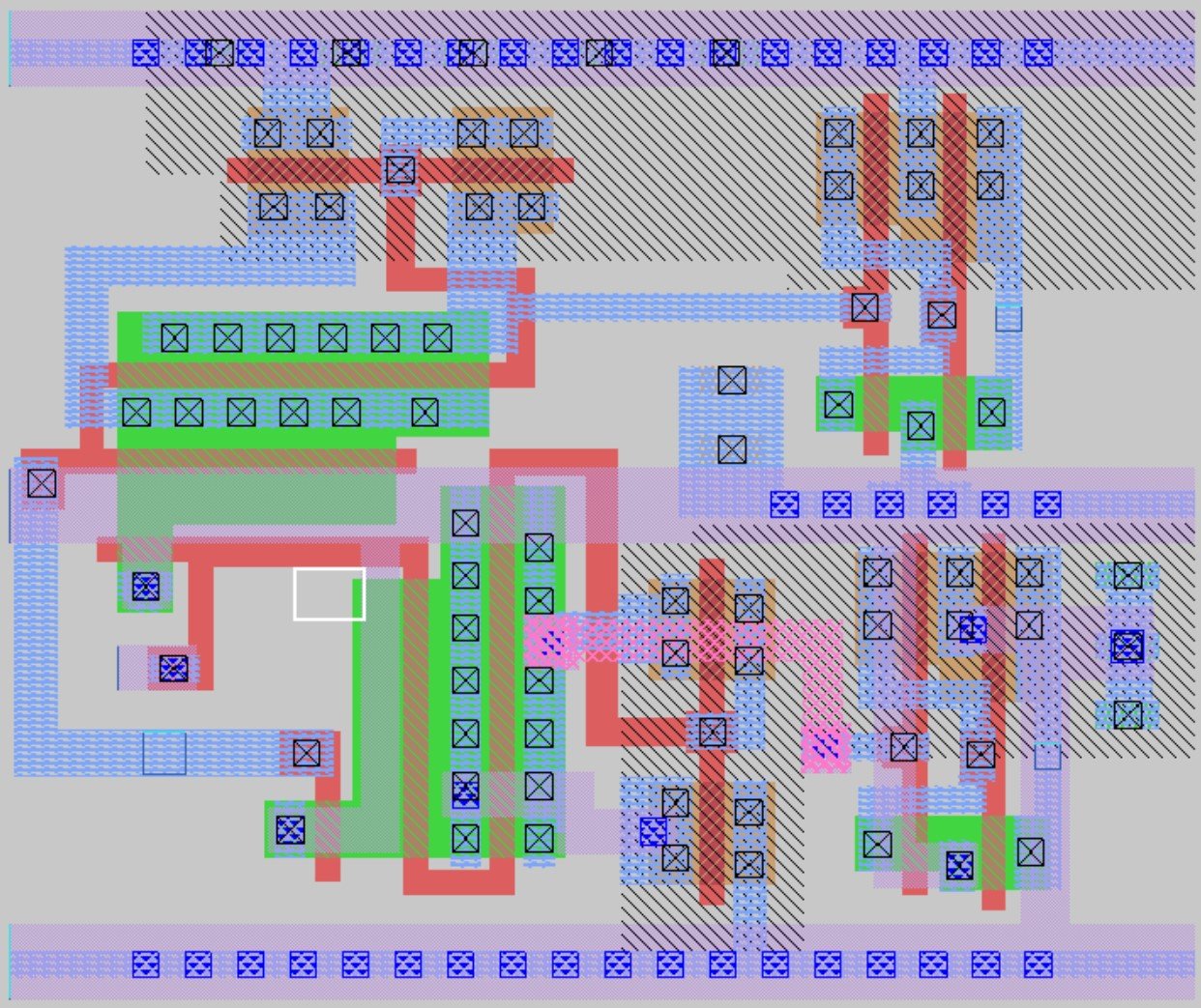
In this interview I talk with Lakshmi S about their shuttle submission.

As well as convering what a PLL is and its component parts, we also answered some interesting questions from the twitter community:
- how long things take to design, what is fun and what is frustrating,
- how to change the PLL’s response,
- why design a integrated loop filter,
- process corners and ngspice
- post silicon testing.
The repository is here.
Interview With Diego Hernando
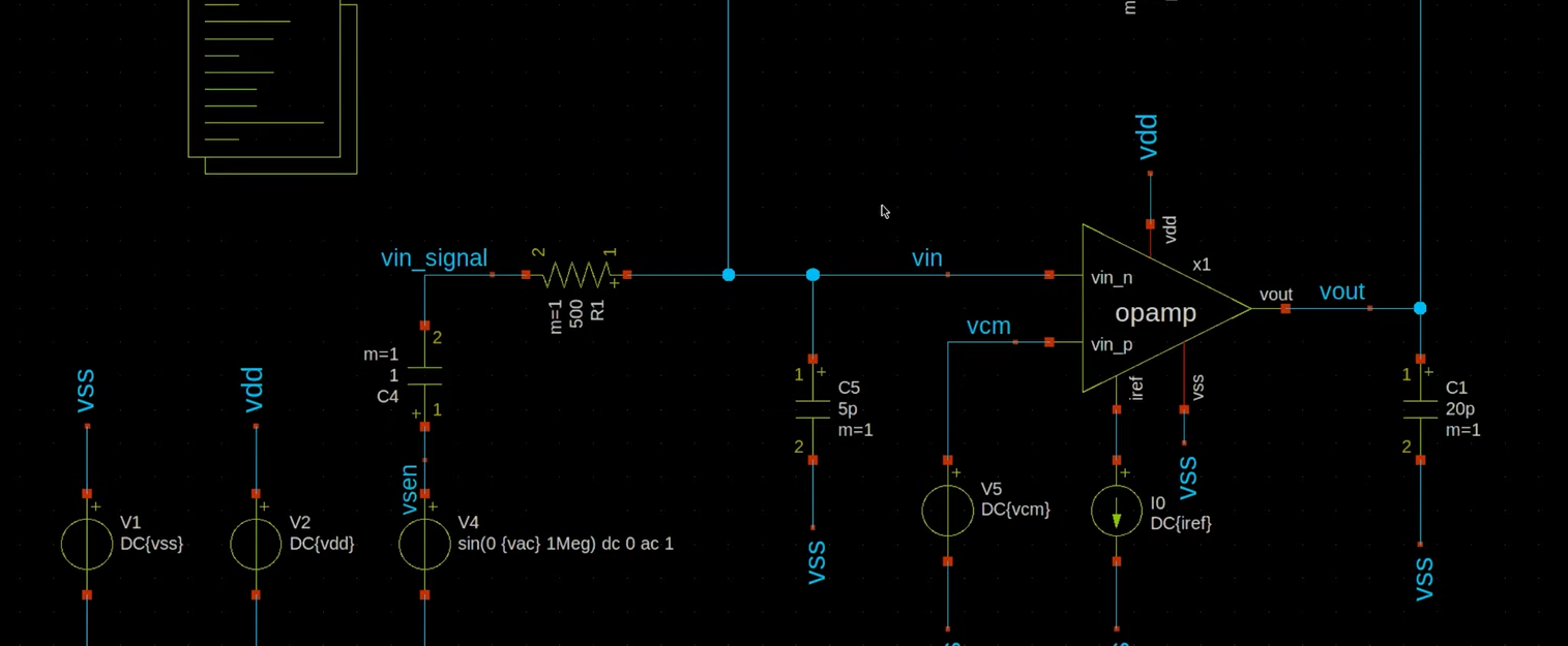
In this interview I talk with Diego Hernando about their ASIC submission.
They have been working on some analog blocks; mostly op-amps but also including a PLL from another designer.
We discuss the difference between digital and analog design, the tools, simulation, layout and testing.
Here’s the link to the repository
Image Attribution
Image attributions for images used on this website.
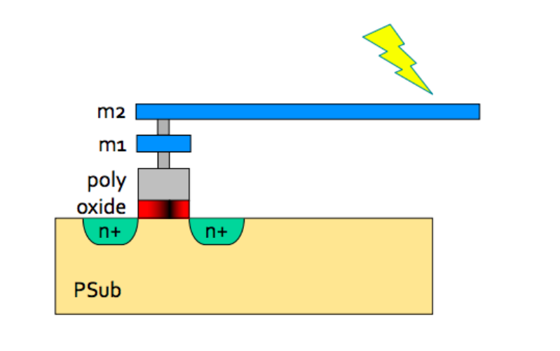 Image from Mohamed Shalan
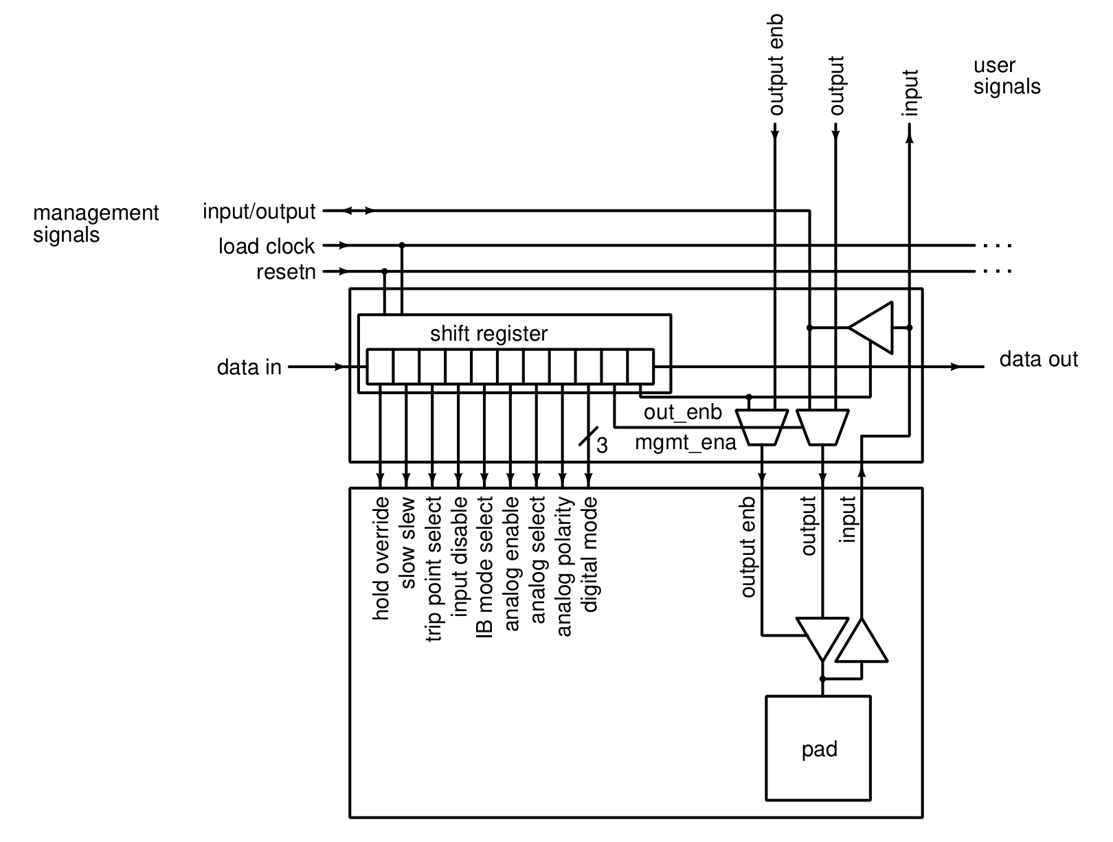 Image from Caravel Datasheet
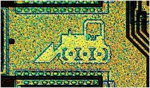 Image from RFCafe
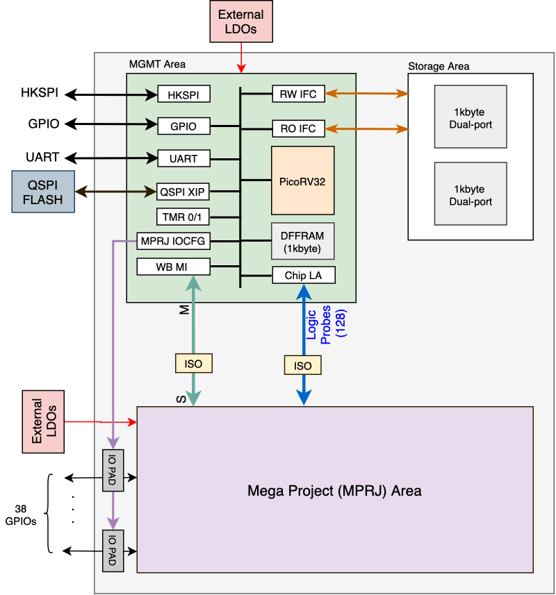 Image from Caravel Datasheet
 Image from Wikipedia
 Image from Components 101
 Image from Wikipedia
 Image from WhaTech
 Image from Technocrazed
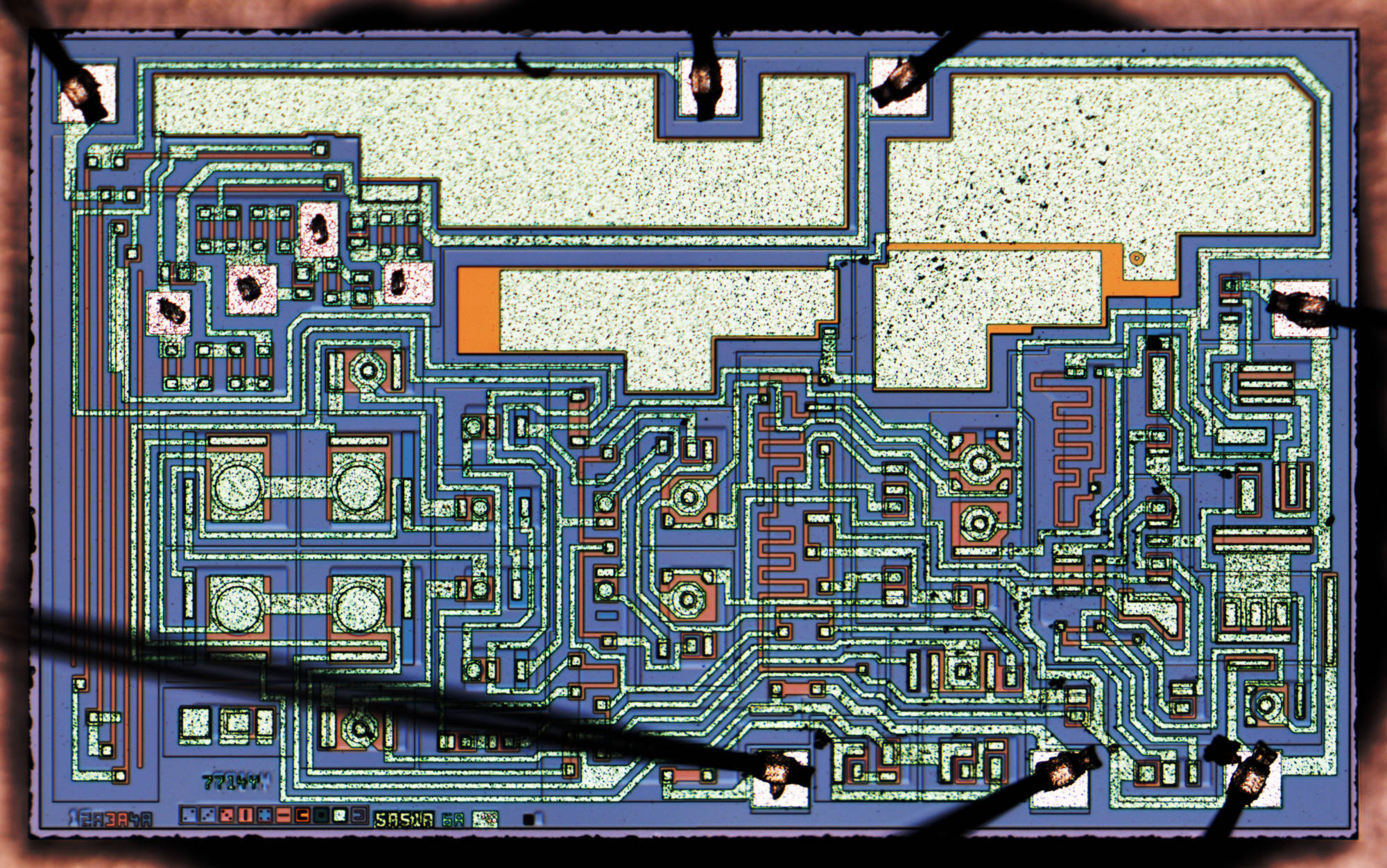 Image from Zeptobars
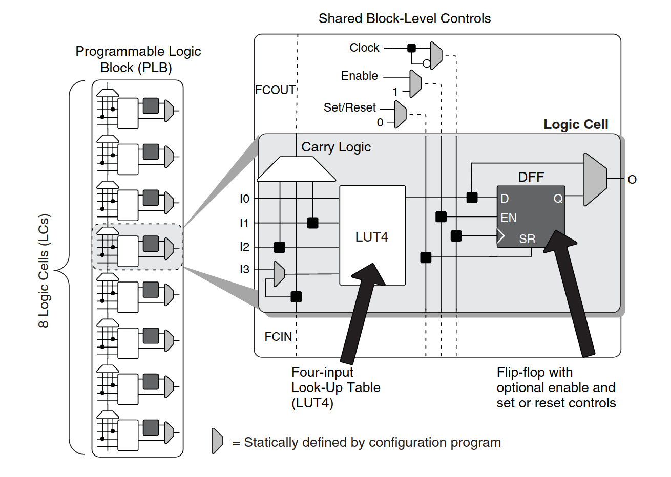 Image from Lattice Semiconductor
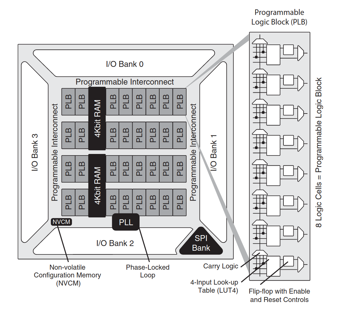 Image from Lattice Semiconductor
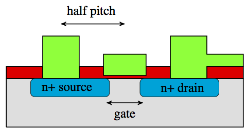 Image from M. Rovitto
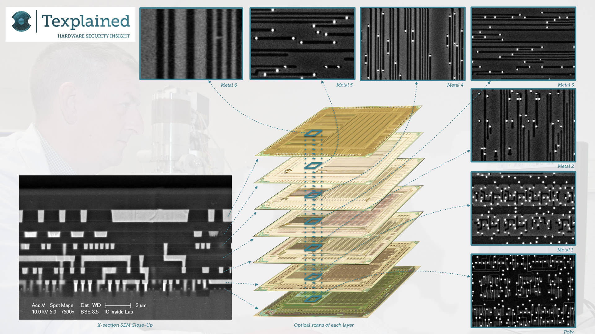 Image from Texplained
My first ASIC - MPW1 submitted
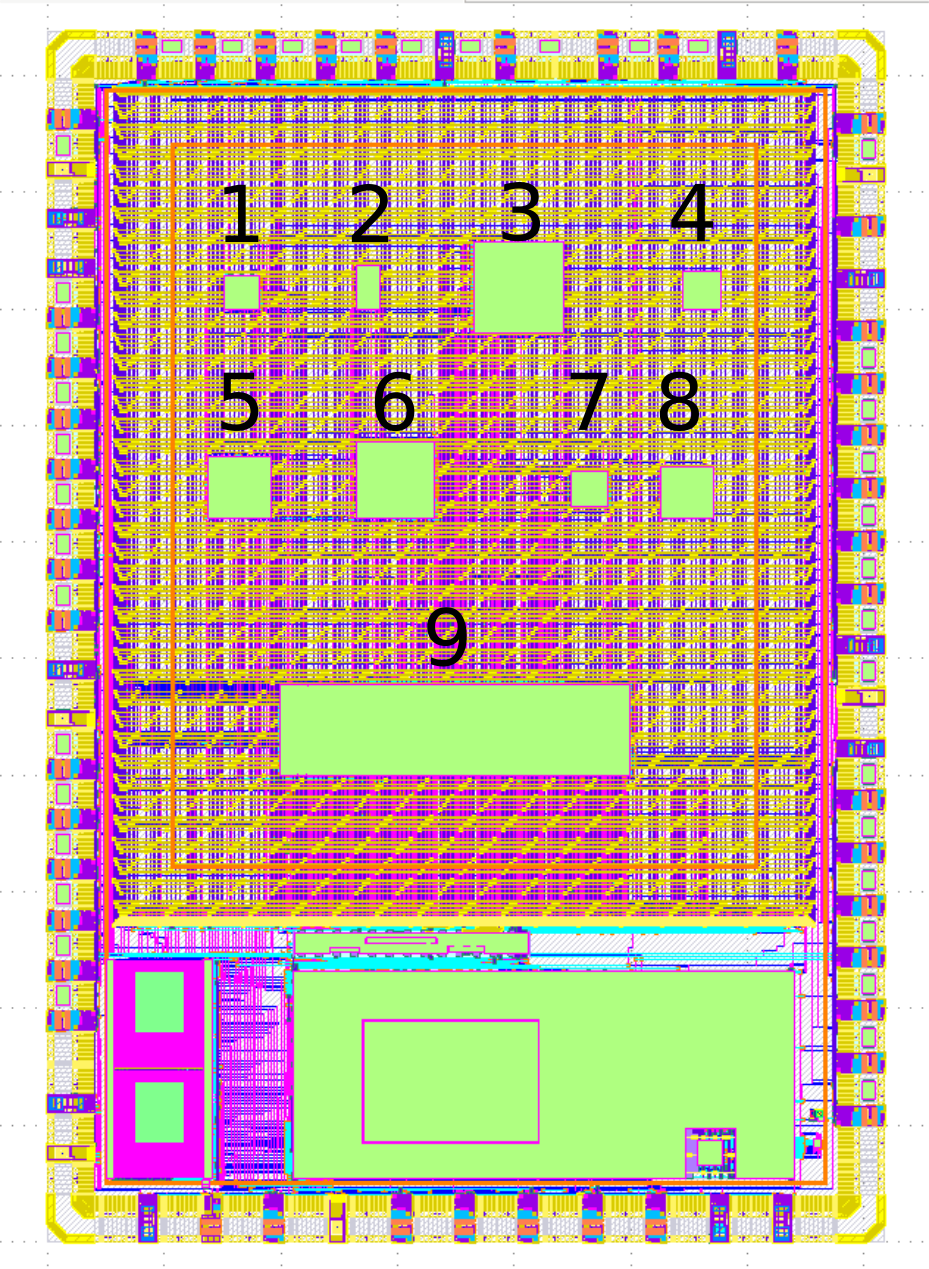
Wow! What a journey. I’m very happy to announce our submission is in and accepted. Now we have a long wait to see if it works! (it does! Jump to the end for an update).
Here’s a picture of the final design. The outer edge and the block at the bottom are all part of Caravel, the standard chip format that everyone on the shuttle has to use. It includes a RISCV processor, RAM, UART, a wishbone bus and more.
Interview with Arya Reais-Parsi - FPGA fabric
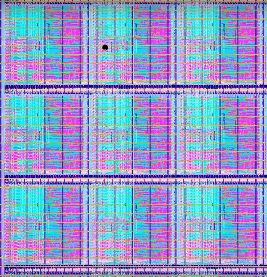
In this interview I talk with Arya Reais-Parsi about their shuttle submission. They are working with a group of students to create Open Source FPGA fabric that can be put on an ASIC and configured with yosys/nextpnr.
The repository is here.
Interview With Sylvain 'tnt' Munaut: USB peripherals
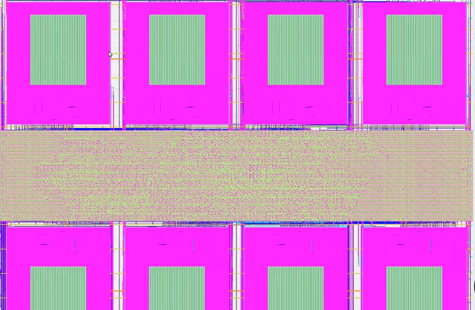
In this interview I talk with Sylvain ’tnt’ Munaut about his Google/Skywater ASIC application.
The design is especially interesting to me because of the way it merges the SRAM blocks with the logic. This has been a major challenge in my own design.
Here’s the link to the repository
Interview With Vladimir Milovanović - spectrometer with Chisel
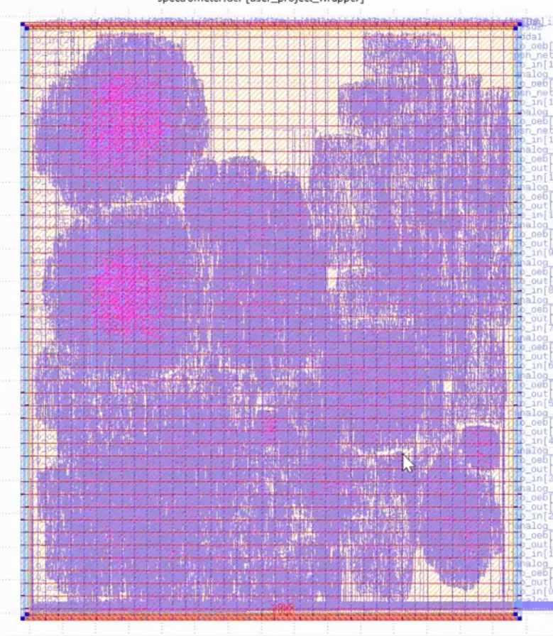
In this interview I talk with Vladimir Milovanović about putting a spectrometer on the Google/Skywater/Efabless ASIC shuttle.
He created the design using Chisel.
The repository is here.
GDS Artwork

I’ve always thought the artwork people put in the top layer of their chips was cool. Do a google image search for chip artwork to see some more fun examples.

While waiting for some toolchain bugs to get ironed out I’ve made a tool to help me make logos. It can take SVG or PNG input and makes a GDS2 file output. These files can then be merged together to create the final layout for the ASIC.
How Much Can We Fit on an ASIC?
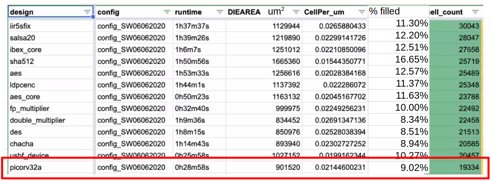
The Google / Skywater shuttle reserves about 10 square mm (10 million square microns) of space for your design.
This comparison that Mohamed from efabless put together shows the various areas (and time to generate the GDS2 files) of some popular designs.

We could fit in about 10 picorv32 RISCV cores!
My designs
I currently have 3 designs ready to add to the multi project harness:
| Name | Square microns | How many would fit? |
|---|---|---|
| seven segment seconds | 10000 | 1000 |
| vga clock | 32400 | 300 |
| ws2812 LED driver | 72900 | 140 |
There is a lot of room for simple designs!
VGA clock
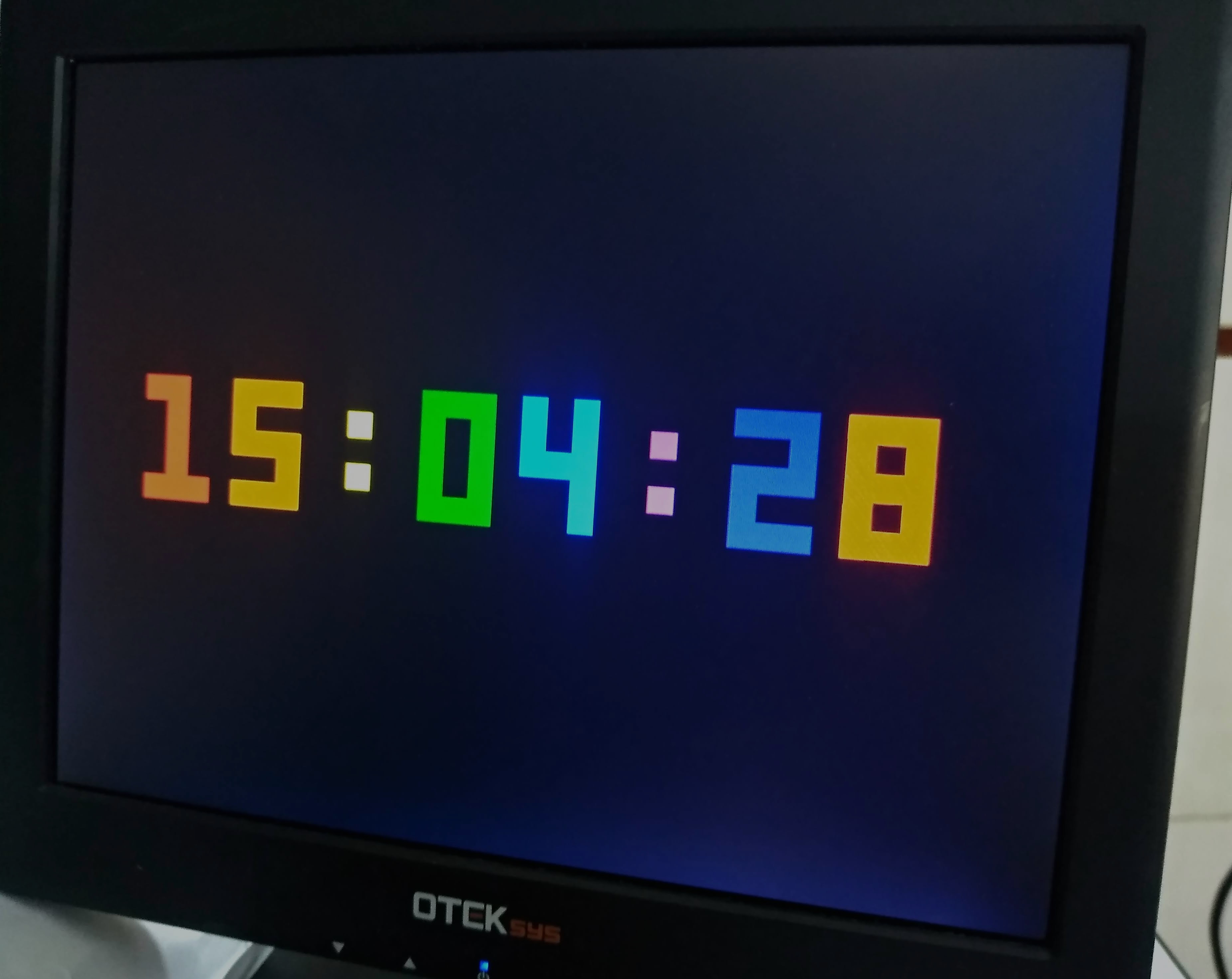
This is one of the first projects I hardened using OpenLane.
News update: my clock works! And you can buy a kit here!
Still can't quite believe I have a clock on my desk that is powered by a chip I designed! pic.twitter.com/O5c2omQYYp
— Matthew Venn (@matthewvenn) March 31, 2022
It shows the time on an LCD panel. It will be part of my first tapeout.
After running the OpenLane ASIC flow, it results in a design that uses 180x180 microns (32000 square microns). As we have about 10e6 square microns in the user project area of the Google shuttle, I could potentially put about 300 of these on the ASIC!