3D Printed Standard Cells
ASICs pack in billions of transistors per square centimeter, making their construction and functionality impossible to understand with the naked eye.
In fact, the upcoming 2 nanometer technology will be so small* that the transistor dimensions will only be 20X larger than an individual atom.
Wouldn’t it be great to see how ASICs are built in 3D at a scale that our bulky human hands can appreciate?
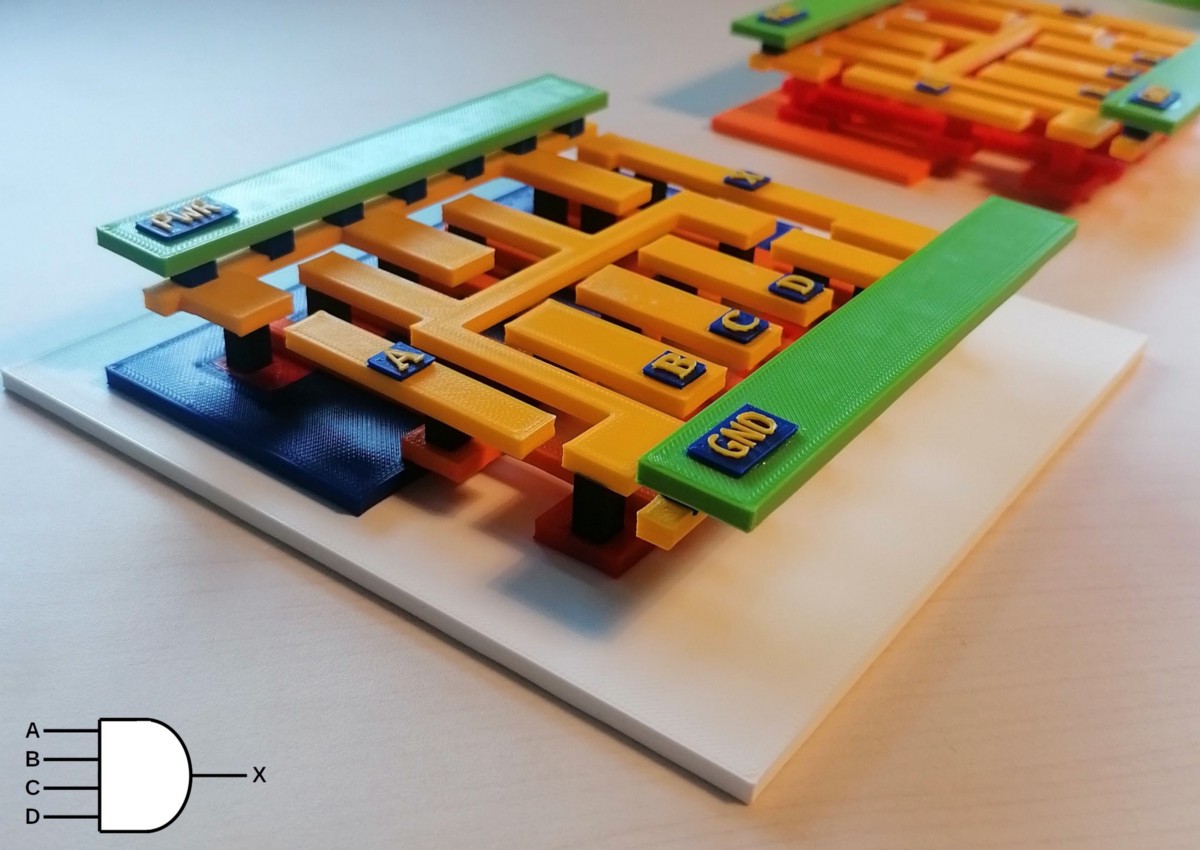
Well wait no longer! Thanks to Thorsten Knoll’s guide, you can now 3D print the cells that make up an ASIC using the GDS files.
 Evolution of ASICs, from Computer History
These 3D structures are an excellent way to visualize how the different metal and silicon layers are combined to create a chip. They also make an excellent accent piece for your office or workshop.
 3D-printed AND gate, courtesy of Thorsten Knoll
In the Zero to ASIC course you will learn how to generate the GDS needed to not only 3D print your design, but also fabricate your chip in silicon. No VLSI, RTL, or prior tapeout experience required.
Interested in chip design but hoping to tackle a smaller project first? Check out Tiny Tapeout. With an easy-to-use a graphical user interface, you can design your own ASIC in less than an evening!
*The dimensions implied by a node’s name (e.g. 2 nm) aren’t entirely truthful. Learn more about CMOS Node Size